CSC/ECE 506 Spring 2013/1d mv
For Reviewers
This section will be removed once reviews are complete. As advised by Dr.Gehringer, here are links to help you compare our work with the older wikis:
- Link to the instruction page: https://docs.google.com/a/ncsu.edu/document/d/1898MW7jXRhuz40HXXiTsobSUDdUVBZ-aUjEyLdeQdNc/edit. Our topic is 1d.
- Link to first wiki written last spring: http://wiki.expertiza.ncsu.edu/index.php/CSC/ECE_506_Spring_2012/1b_as
- Link to second wiki written last spring: http://wiki.expertiza.ncsu.edu/index.php/CSC/ECE_506_Spring_2012/1b_ps
What is Moore's Law?
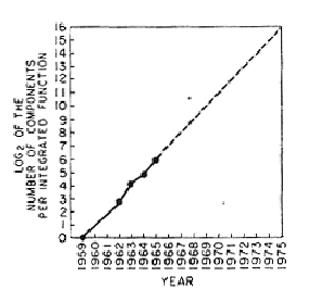
Moore's Law, named after Gordon Moore, co-founder of Intel, states that the number of transistors that can be placed on an integrated circuit will double approximately every two years<ref>http://www.computerhistory.org/semiconductor/timeline/1965-Moore.html</ref>. The original prediction in 1965 stated a doubling every 12 months but, in 1975, after microprocessors were introduced that were less dense than originally predicted, he slowed the rate of doubling to it's current rate of two years <ref>http://arstechnica.com/hardware/news/2008/09/moore.ars</ref>. Instead of giving an empirical formula predicting the rate of increase, Moore instead used prose, graphs, and images to convey these predictions and observations to the masses. This, in some ways, increased the staying power of Moore's Law, allowing the industry to use it as a benchmark of success and a measurable determination of their success. Virtually all digital devices are in some way fundamentally linked to the growth set in place by Moore's Law.<ref>http://en.wikipedia.org/wiki/Moore's_Law</ref>
Historical context

One of the first reviews of progress in the semiconductor industry was written by Moore, for the 35th anniversary issue of Electronics Magazine in 1965 <ref> http://download.intel.com/museum/Moores_Law/Articles-Press_Releases/Gordon_Moore_1965_Article.pdf </ref>. After only six years since the introduction of the first commercial planar transistor in 1959, Moore observed an astounding trend: the number of components per chip was roughly doubling every year, reaching about 64 components in 1965. Extrapolating this trend for a decade, Moore predicted that chips with 65,000 components would be available by 1975. In 1975, Moore revisited his 1965 prediction and provided some critical insights into the technological drivers of the observed trends <ref>http://ieeexplore.ieee.org/xpls/abs_all.jsp?arnumber=1478174</ref>. Moore divided the advances in circuit complexity among its three principle technical drivers: increasing chip area, decreasing feature size, and improved device and circuit designs. Minimum feature sizes were decreasing by about 10% per year (resulting in transistors that were about 21% smaller in area, and an increase in transistors per area of 25% each year). Chip area was increasing by about 20% each year. These two factors alone resulted in a 50% increase in the number of transistors per chip each year. Design cleverness (eliminating nonfunctional chip area) made up the rest of the improvement (33%). By breaking the devise improvement into its three technology driver constituents, Moore was able to extrapolate each trend and predict a change in the slope of his observation. Moore saw that progress in lithography was allowing a continued decrease in the size of architectural features to one micrometer or less. Continued reductions in defect density and increases in wafer size allowed the die area trend to continue. Although improvements in device isolation and the development of the metal-oxide-semiconductor transistor had contributed to greater packing density, Moore saw the latest circuits as approaching their design limits. Seeing an end to the design cleverness trend in four or five years, Moore predicted a change in the slope of his trend from doubling every year, to doubling approximately every 18 months. Beginning in 1979, the industry followed the new Moore’s Law trend throughout the 1980s and early-1990s.
By the late-1970s, another interesting trend emerged: the bifurcation of Moore’s Law into memory and logic trend lines. While memory chips continued to advance at the Moore’s Law complexity limit, logic chips (such as microprocessors) advanced at a slower pace <ref>G. E. Moore, “VLSI: Some fundamental challenges,” IEEE Spectrum, vol. 16, no. 4, pp. 30–37, Apr. 1979. </ref> . In essence, the ability to put more transistors on a chip outstripped the ability to design chips with that many transistors for a market need. This split of Moore’s Law in two persisted for the next two decades, where by the year 2000 memory chips used 1 billion transistors, but advanced microprocessors had only 20–40 million transistors. While memory chips increased their transistors per chip by 1.58X per year, microprocessors saw only a 1.38X per year increase <ref>http://www.icknowledge.com/products/reports.html</ref>.
Semiconductor devices in computer hardware
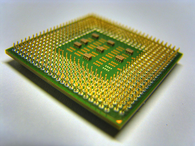
Computer hardware has three basic components - a processor that rapidly executes instructions, memory that stores vast quantities of instructions and data (for instructions to manipulate), and input/output devices (like keyboards, displays, and interfaces to networks) that connect a computer to the outside world. Hardware designers seek to make processors execute instructions faster, memory provide information faster, and input/output devices that communicate faster. These electronic components are implemented on a semiconductor-based integrated circuit.
A semiconductor is a solid-state electronic device which can be switched to conduct or block electric currents <ref>http://research.microsoft.com/en-us/um/people/gray/moore_Law.html</ref>. Semiconductors can be divided into two main groups: integrated circuits and discrete devices. Integrated circuits (ICs) consist of many active and passive elements that are fabricated and connected together in a single chip. ICs can be further broken down into digital or analog devices. Digital ICs store and process information expressed in binary numbers or "bits". They perform arithmetical operations or logical functions by manipulating binary signals.
Today, it is most common to implement a processor on a single silicon chip called a microprocessor. A microprocessor is an IC which provides on one chip functions equivalent to those contained in the processing unit of a computer. A microcontroller is a microprocessor and memory integrated on the same chip and is used in dedicated applications such as traffic signals, laser printers, or antilock brakes in automobiles. Microperipheral devices accompany microprocessors to handle a computer's related function such as graphics. Logic chips handle the mathematical treatment of formal logic by translating AND, OR, and NOT functions into a switching circuit, or logic gate. This category includes application-specific ICs (ASICs) including gate arrays, standard cells, and programmable logic devices (PLDs). Most computers today employ a single microprocessor, but large computers use several microprocessors (and, in a few cases, thousands).
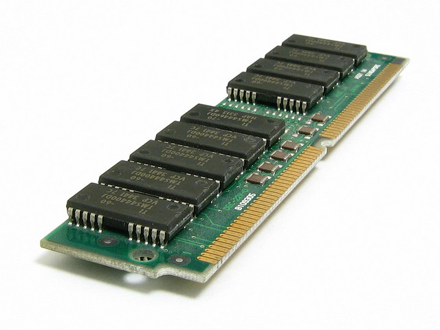
Semiconductor memory devices store information in the form of electrical charges. Memory devices can be subdivided into volatile and non-volatile families. The Random-Access Memory ([RAM) is a volatile memory product, which means it will lose stored information (charges) once power is turned off. This product sub-category includes the popular DRAM (Dynamic RAM) and, to a lesser degree, the SRAM (Static RAM). In contrast, non-volatile memory products retain information even after power is turned off. Non-volatile memory includes the ROM (Read Only Memory) and its "erasable" derivatives, the EPROM (Erasable Programmable ROM) and EEPROM (Electrically EPROM). In an EPROM, stored information is erased by exposure to ultraviolet light, whereas the EEPROM has the convenience of selective erasure of information through electrical impulses rather than exposure to ultraviolet light. Flash Memory is an IC which has the ability to bulk erase its entire contents simultaneously. It shares the advantage of other non-volatile memory in that it retains information when power is turned off. Current desktop computer memories are implemented in several chips and backed up by one or more magnetic disks. Larger computers can employ hundreds of memory chips and disks.
Manufacturing techniques
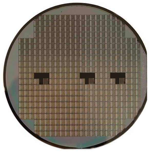
At the heart of Moore's Law is the transistor. Computer chips contain hundreds of millions of transistors embedded on a wafer of silicone. To make these chips, first a stencil is made containing the outlines of millions of transistors. The stencil is then placed over a silicone wafer which is sensitive to ultraviolet light. The light penetrates through the gaps of the stencil and exposes the silicon wafer, which is then is bathed in acid, carving the outlines of the circuits and the design of millions of transistors. Since the wafer consists of many conducting and semiconducting layers, the acid cuts into the wafer at different depths and patterns, so one can create circuits of enormous complexity.
One reason why Moore’s Law has relentlessly increased the power of chips is because UV light can be tuned so that its wavelength is smaller and smaller, making it possible to etch increasingly tiny transistors onto silicon wafers. Since UV light has a wavelength as small as 10 nanometers, the smallest transistor that can be etched is about thirty atoms across.<ref>http://en.wikipedia.org/wiki/Photolithography</ref> Due to physical limitations, This process cannot go on forever. At some point, it will be physically impossible to etch smaller effective transistors, and Moore’s Law as we understand it will finally collapse.
Currently, estimates predict that around 2020 or soon afterward, Moore’s Law will gradually cease to hold true for traditional transistor technology. Transistors will be so small that quantum effects will begin to take over and electrons will "leak" out of the wires.<ref>http://computer.howstuffworks.com/small-cpu2.htm</ref><ref>http://www.monolithic3d.com/2/post/2011/09/is-there-a-fundamental-limit-to-miniaturizing-cmos-transistors1.html</ref> For example, the thinnest layer inside a computer will be about five atoms across. At that size, quantum effects will become dominant and transistors will not function as they currently do without other technological advances.
A common misconception
Moore's Law is often linked to performance improvements as measured in CPU clock speeds. In the 1980's, former Intel executive David House stated that chip performance would double every 18 months.<ref>http://news.cnet.com/Myths-of-Moores-Law/2010-1071_3-1014887.html</ref> This is a consequence of Moore's Law, but it is not what Moore's Law actually claims. In fact, due to heat dissipation issues<ref>http://www.gotw.ca/publications/concurrency-ddj.htm</ref><ref>http://techtalk.pcpitstop.com/2007/08/06/cpu-clock-speeds/</ref>, performance as measured in clock speed has remained flat since 2005<ref>http://www.kmeme.com/2010/09/clock-speed-wall.html</ref> while the number of transistors continues to double roughly every 2 years.
Moore's Law, past to present

Reviewing data from the inception of Moore's Law to the present shows that, consistent to Moore's prediction, the number of transistors on a chip has doubled approximately every 2 years. There are several contributing factors, that had they not been developed, could have slowed or halted Moore's Law. One of these is the invention DRAM. The main advantage of DRAM over its predecessor, SRAM, is that only one transistor and a capacitor are required per bit, compared to four or six transistors with SRAM. Another is most certainly the CMOS technology. This allowed a higher density of logic functions on a chip with the added benefit of low power consumption and electrical noise immunity. Lastly was the invention of the integrated circuit itself. Moore's Law isn't only predictive pf making larger and faster chips, but also smaller, cheaper, and more efficient ones as well.
As visible in the examples below, Moore's Law has seemed to hold at an overall exponential rate of growth consistent to what Moore predicted. There is some variation from year to year that can be explained by the introduction of new technology or manufacturing techniques that helped kick-start Moore's Law back on trend. This is most evident with the "Dual-Core Itanium 2" processor. It was ahead of it's competitors by a full four years. The example to the right showes a dip in transistor count during 1995-2003. This is balanced out by an almost equal increase in the following eight years.
| Processor | Transistor count | Date of introduction | Manufacturer | Process | Area |
|---|---|---|---|---|---|
| Intel 4004 | 2,300 | 1971 | Intel | 10 µm | 12 mm² |
| Intel 8008 | 3,500 | 1972 | Intel | 10 µm | 14 mm² |
| MOS Technology 6502 | 3,510 | 1975 | MOS Technology | 21 mm² | |
| Motorola 6800 | 4,100 | 1974 | Motorola | 16 mm² | |
| Intel 8080 | 4,500 | 1974 | Intel | 6 μm | 20 mm² |
| RCA 1802 | 5,000 | 1974 | RCA | 5 μm | 27 mm² |
| Intel 8085 | 6,500 | 1976 | Intel | 3 μm | 20 mm² |
| Zilog Z80 | 8,500 | 1976 | Zilog | 4 μm | 18 mm² |
| Motorola 6809 | 9,000 | 1978 | Motorola | 5 μm | 21 mm² |
| Intel 8086 | 29,000 | 1978 | Intel | 3 μm | 33 mm² |
| Intel 8088 | 29,000 | 1979 | Intel | 3 μm | 33 mm² |
| Intel 80186 | 55,000 | 1982 | Intel | ||
| Motorola 68000 | 68,000 | 1979 | Motorola | 4 μm | 44 mm² |
| Intel 80286 | 134,000 | 1982 | Intel | 1.5 µm | 49 mm² |
| Intel 80386 | 275,000 | 1985 | Intel | 1.5 µm | 104 mm² |
| Intel 80486 | 1,180,000 | 1989 | Intel | 1 µm | 160 mm² |
| Pentium | 3,100,000 | 1993 | Intel | 0.8 µm | 294 mm² |
| AMD K5 | 4,300,000 | 1996 | AMD | 0.5 µm | |
| Pentium II | 7,500,000 | 1997 | Intel | 0.35 µm | 195 mm² |
| AMD K6 | 8,800,000 | 1997 | AMD | 0.35 µm | |
| Pentium III | 9,500,000 | 1999 | Intel | 0.25 µm | |
| AMD K6-III | 21,300,000 | 1999 | AMD | 0.25 µm | |
| AMD K7 | 22,000,000 | 1999 | AMD | 0.25 µm | |
| Pentium 4 | 42,000,000 | 2000 | Intel | 180 nm | |
| Atom | 47,000,000 | 2008 | Intel | 45 nm | |
| Barton | 54,300,000 | 2003 | AMD | 130 nm | |
| AMD K8 | 105,900,000 | 2003 | AMD | 130 nm | |
| Itanium 2 | 220,000,000 | 2003 | Intel | 130 nm | |
| Cell | 241,000,000 | 2006 | Sony/IBM/Toshiba | 90 nm | |
| Core 2 Duo | 291,000,000 | 2006 | Intel | 65 nm | |
| AMD K10 | 463,000,000 | 2007 | AMD | 65 nm | |
| AMD K10 | 758,000,000 | 2008 | AMD | 45 nm | |
| Itanium 2 with 9MB cache | 592,000,000 | 2004 | Intel | 130 nm | |
| Core i7 (Quad) | 731,000,000 | 2008 | Intel | 45 nm | 263 mm² |
| Six-Core Xeon 7400 | 1,900,000,000 | 2008 | Intel | 45 nm | |
| POWER6 | 789,000,000 | 2007 | IBM | 65 nm | 341 mm² |
| Six-Core Opteron 2400 | 904,000,000 | 2009 | AMD | 45 nm | 346 mm² |
| 16-Core SPARC T3 | 1,000,000,000 | 2010 | Sun/Oracle Corporation|Oracle | 40 nm | 377 mm² |
| Core i7 (Gulftown) | 1,170,000,000 | 2010 | Intel | 32 nm | 240 mm² |
| 8-core POWER7 | 1,200,000,000 | 2010 | IBM | 45 nm | 567 mm² |
| z196 | 1,400,000,000 | 2010 | IBM | 45 nm | 512 mm² |
| Dual-Core Itanium 2 | 1,700,000,000 | 2006 | Intel | 90 nm | 596 mm² |
| Tukwila | 2,000,000,000 | 2010 | Intel | 65 nm | 699 mm² |
| Core i7 (Sandy Bridge-E) | 2,270,000,000 | 2011 | Intel | 32 nm | 434 mm² |
| Nehalem-EX | 2,300,000,000 | 2010 | Intel | 45 nm | 684 mm² |
| 10-Core Xeon Westmere-EX | 2,600,000,000 | 2011 | Intel | 32 nm | 512 mm² |
| 8-Core AMD Bulldozer | 1,200,000,000 | 2012 | AMD | 32nm | 315 mm² |
| Quad-Core + GPU AMD Trinity | 1,303,000,000 | 2012 | AMD | 32 nm | 246 mm² |
| Quad-Core + GPU Core i7 | 1,400,000,000 | 2012 | Intel | 22 nm | 160 mm² |
| 8-core POWER7+ 80M L3 | 2,100,000,000 | 2012 | IBM | 32 nm | 567 mm² |
| Six-core zEC12 | 2,750,000,000 | 2012 | IBM | 32 nm | 597 mm² |
| 8-Core Itanium Poulson | 3,100,000,000 | 2012 | Intel | 32 nm | 544 mm² |
| 62-Core Xeon Phi | 5,000,000,000 | 2012 | Intel | 22 nm |
Rock's law: The lesser known second law
There is another fundamental principle known as Rock's Law. This law is a direct consequence to Moore's law in that the cost to produce transistors on a chip may go down, these costs instead flow towards manufacturing, testing, and research and development. The law states that the cost of a semiconductor chip fabrication plant doubles ever four years. Simply put, in order for Moore's law to hold, Rock's law must also hold.<ref>http://en.wikipedia.org/wiki/Rock%27s_Law</ref>
Effect of Moore’s Law
Industry roadmaps
Over the years, predictions of future industry performance reached such a level of acceptance that they have been codified in industry-sanctioned “roadmaps” for the future. The National Technology Roadmap for Semiconductors (NTRS) was first developed by the Semiconductor Industry Association (SIA) <ref> http://www.sia-online.org/ </ref> in 1994 to serve as an industry standard of Moore’s Law. It extrapolated then-current trends to the year 2010, where 70 nm minimum feature sizes were predicted to enable 64 Gigabytes of DRAM chip production. This official industry roadmap has been updated many times, going international in 1999 to become the International Technology Roadmap for Semiconductors (ITRS) <ref>http://public.itrs.net/</ref>. By enshrining it in a major planning document, these road maps have turned Moore’s Law from a prediction for the future into a commitment for the semiconductor industry. These road maps described the lock-step industry progression along technological nodes, provided common terminology to suppliers and customers of the semiconductor industry, and attempted to describe the major challenges to continued progress along Moore’s Law.
Computing innovation
An enormous impact of Moore’s Law was to dramatically constrain and focus the computer industry <ref>http://www.ieee.org/portal/site/sscs/index.jsp?pageID=sscs_enews_home&month=09&year=2006</ref>. For decades, before the advent of significant levels of integration in semiconductors, innovations in computer architecture formed the basis of competition among vendors. These innovations meant that system organization, instruction sets, memory management techniques and I/O controllers were different in every product generation and from every vendor. Before System 360, introduced in 1964 by IBM <ref>http://en.wikipedia.org/wiki/IBM_System/360</ref>, there had hardly been two consecutive models that were compatible. These dramatic changes in direction meant that no particular design ever had enough customers to become low in cost, or to allow a meaningful independent software industry to arise.
Moore’s Law raised the velocity of cost/performance improvement far above maneuvering speed for the computer industry. That is, the tremendous rate of improvement in cost/performance via feature size reduction made it unwise for computer vendors to attempt architectural changes, which meant in turn that the semiconductor suppliers took control of the architecture of their customers’ designs by integrating more function in their chips, running them faster, and reducing electronic costs steadily.
This, in turn, meant that these high performance and low cost processors and memories were available to all incumbent computer vendors and to industry newcomers as well. Over a fifteen year period, the existing computer industry was commoditized, and slowly destroyed. Even IBM was forced to transform itself further in the direction of providing services and to concentrate its own architectural efforts in the very top of the market. But this brave new world proved very hospitable to low cost manufacturers, who concentrated their efforts on power and packaging and distribution, taking out costs and improving reliability and relying on Intel, AMD or Motorola for the major value creation.
A huge collateral effect of Moore’s Law was the creation of the commercial software industry as a meaningful force in the economy. This took place in two ways. First, the falling cost and wide availability of powerful processors greatly increased the number of computers in use, and thus successful software products could be sold in enormous numbers at modest prices. Secondly, the end of proliferation of architectural variations meant that a successful software product need run on only one or at most two different CPU types, secure in the knowledge that (a) this would cover virtually the entire market of all vendors and customers, and (b) that there would be inexorable steady improvements in cost/performance which would seldom require any significant changes to the programs, thus allowing larger software investments to be made, in products which would surely perform better and better over time, courtesy of Moore’s Law.
Economic impact
The economic drivers for Moore’s Law have been extraordinarily compelling. As the dimensions of a transistor shrank, the transistor became smaller, lighter, faster, consumed less power, and in most cases was more reliable. All of these factors made the transistor more desirable for virtually every possible application. Historically, the semiconductor industry has been able to manufacture silicon devices at an essentially constant cost per area of processed silicon. Thus, as the devices shrank they enjoyed a shrinking cost per transistor. This new capability (either due to an increase in performance or a decrease in cost, or both) created new markets for the product, which increased the volume of sales. Higher sales volumes allowed a percentage of those sales to be reinvested in the development of the next technology evolution. Even though each technology generation requires an increasing investment for development, the higher sales volume driven by the newly enabled markets justified the investment.
Limitations of Moore's law
Moore’s law has long been known to have a limit. Even Moore himself stated in an interview that exponentials cannot be maintained indefinitely. In terms of transistor size and processing speed, the limits can be seen 10 to 20 years in the future. The limitations are often attributed to the physical limits of individual transistors. In 2003, Intel predicted that the limitation would come sometime between 2013 and 2018 with the advent of 16 nanometer manufacturing processes and 5 nanometer gates. Intel said that, at these scales, Quantum Tunneling effects would cause electrons flowing through transistors to unpredictably tunnel out of the constraining transistors, thus losing both efficiency and information. Even in these cases, the theoretical limits are still much more powerful. Lawrence Krauss and Glenn D. Starkman stated a limit would be reached nearly 600 years in the future. This was based on rigorous estimation of total information-processing capacity of any system in the Universe, which is limited by the Bekenstein bound. Assuming that Quantum Tunneling and other effects can be overcome, what systems then will perpetuate Moore’s law?
Beyond Moore's law
There are a few new technologies that have the potential to change the underlying architecture of processors and extend performance gains past the theoretical limits of traditional transistors. These new architectures include some of the newest advancements in computer engineering, and some which are currently only theoretical.
Does transistor count matter?
Moore's Law concerns only the doubling of transistors on the same die space every 2 years. While some of these new technologies deal directly with adding more transistors into the same amount of space, others take a different approach to boost overall computational performance. While not strictly following Moore's Law, per se, these advanced designs will lead to a continuation of the increase in computational power that can be harnessed from hardware. Novel approaches, such as 3-D transistor manufacturing allow for greater densities, but other approaches, such as quantum computing operate in a different way than the traditional transistor to solve the same problem more efficiently.<ref>http://www.monolithic3d.com/2/post/2011/09/is-there-a-fundamental-limit-to-miniaturizing-cmos-transistors1.html</ref><ref>http://www.iue.tuwien.ac.at/phd/wittmann/node6.html</ref>
The Memristor
The memristor, currently being developed by Hewlett Packard, is a new type of transistor that combines both electrical charge and magnetic flux. As current flows in one direction through the circuit, resistance increases. Reversing the flow will decrease the resistance and stopping the flow will leave the resistance in the current state. This type of structure allows for both data storage and data processing (logic gate construction). Memristors can be layered in three dimensions on silicone, yielding data and transistor densities of up to 1000 times greater than currently available. HP has reported the ability to fit 100 gigabytes in a square centimeter [1] and with the ability to layer memristors, this could lead to pocket devices with a capacity of over 1 petabyte. in 2012 HP integrated memristors with existing CMOS architectures to create the first working memristor computer. Future integration and layering of memristors points to the ability to compute along a 3d structure instead of mainly 2d structures. Since current processors operate in 2 dimensions (except for a few vertically integrated designs), memristors could effectively square the computing power of a chip without considering how much faster a memristor system is than a traditional transistor based approach.
Quantum computing
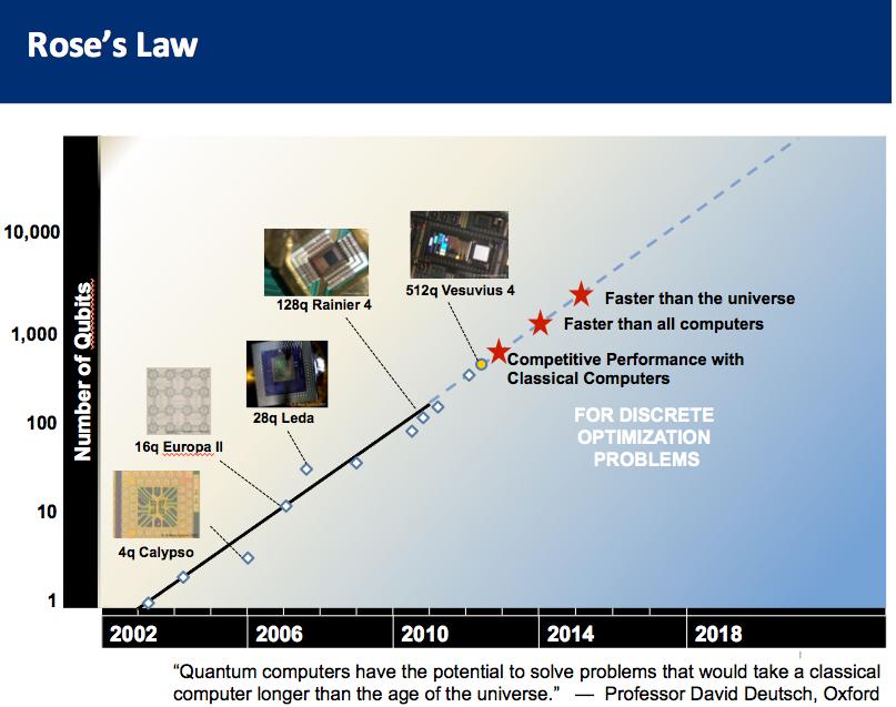
Quantum computing works by essentially allowing all available bits to enter into superposition. Using this superposition, each "q-bit" can be entangled with other q-bits to represent multiple states at once. By using quantum logic gates, the qbits can be manipulated to find the desired state among the superposition of states. This has great potential for drastically shortening the time necessary to solve several important problems, including integer factorization and the discrete logarithm problem, upon which much current encryption is based. Quantum computing faces several technical issues, including decoherence, which makes quantum computers difficult to construct and maintain. But assuming that these technical issues can be overcome, how do we determine the speedup from traditional computing? The so called Rose’s Law at right gives us a good idea.
Like Moore’s Law, a straight line describes an exponential. But unlike Moore’s Law, the computational power of the quantum computer should grow exponentially with the number of entangled quantum bits as well. This means that if you double the amount of transistors for a quantum machine in one year, you effectively square the processing power. This increase in speed could theoretically reach faster than all current computers combined computational speed.
Ballistic Deflection Transistors
Ballistic deflection transistors are another promising avenue of re-design for the traditional transistor. Essentially, single electrons are passed through a transistor and deflected into one path or the other, thus delivering a 0 or a 1. The theoretical speed of these transistors is in the terahertz range[16]. Current processing speeds of CPU’s have stalled around 3.5 Gigahertz. This means that ballistic deflection transistors could increase the range of Moore’s law for around a decade or more.
Other technologies
The arena of research to produce an alternative to the traditional transistor includes many novel approaches. They include (but are not limited to):
- Optical Computing
- DNA Computing
- Molecular Electronics
- Spintronics
- Chemical Computing
- Artificial Neural Networks
- Unconventional Computing
Conclusions
The demise of Moore's Law has been predicted several times during the past 40 years, but transistor counts continue to follow a two year doubling on average. With the traditional transistor approach, inevitable physical limits will be reached around the 16 nm process, due to quantum tunneling<ref>http://news.cnet.com/2100-1008-5112061.html</ref>. If this is true, the current pace of innovation would lead to hitting "Moore's Wall" around 2022, or in about 10 years. This "10 year horizon" for Moore's Law has existed since the early 1990's, with new designs, processes, and breakthroughs which continue to extend the timeline.<ref>http://arxiv.org/pdf/astro-ph/0404510v2.pdf</ref><ref>http://java.sys-con.com/node/557154</ref> New technologies that leverage three dimensional chip architecture would allow for years of continued growth in transistor counts and exotic designs could further increase the theoretical capacity of transistors in a particular space. If the past is used as a predictor for future trends, it is safe to say that the end of Moore's Law "is about 10 years away".
On another note, if we relax the definition of Moore's Law to include computational performance gains, we open a whole new avenue by which to measure computing power. Most of the easy gains in performance related to transistor counts have been realized, but new designs of how basic computing is performed can theoretically yield large increases in performance without doubling of transistor counts or extremely high power requirements.<ref>http://abcnews.go.com/Technology/story?id=4006166&page=1#.TzAbDcVA_H4</ref><ref>http://www.gotw.ca/publications/concurrency-ddj.htm</ref> The era of the traditional transistor is not quite over yet, but the relevance of transistor counts may be nearing it's end.
See also
- Amdahl's law
- Metcalfe's law
- Exponential growth
- History of computing hardware (1960s–present)
- Quantum computing
- Rock's law
- Semiconductor
- Integrated Circuit
Quiz
- What does Moore's Law imply?
- Transistor placed on IC will double every 18 months
- Speed of processors will double every 18 months
- Speed of memory chips will double every 18 months
- All of the above
- Moore's Law is a ..... ?
- Physical phenomena
- Economic model
- Prediction of technology evolution
- All of the above
- A semiconductor device ..... ?
- Can blocks electricity
- Can conduct electricity
- Is a solid-state device
- All of the above
- Which one of the following is not a type of Random Access memory device?
- DRAM
- EEPROM
- Magnetic disk
- SRAM
- CMOS technology is used in ..... ?
- Building a compiler
- Constructing ICs
- Building a memristor
- Building a quantum computer
Answers
1: 1; 2: 3; 3: 4; 4: 3; 5: 2
References
<references/>