CSC/ECE 506 Spring 2012/6b pa
Introduction
Processors with Write through caches often employ write buffers hide the write latency to the next level of memory hierarchy so that in the case of write misses, the processor does not need to wait until the write is completed as it is not asking for any data. Thus, instead of stalling the processor, we can do the write action in the background, write the data into a write buffer and delegate the responsibility to the write buffer for performing the write to the memory hierarchy. In a shared memory multiprocessor, there are more advantages to buffer these memory requests as they help reducing the memory processor interconnection traffic as each access needs to compete with memory requests from different processors. The main memory bandwidth of the shared memory systems is an important factor that affects the performance of the shared memory systems. This is because the off-chip bandwidth is low. A large number of writes to the main memory can lead to slower systems that need to wait for 100s of cycles until the slow main memory subsystem finishes the whole write access.
Concerns of Write Buffers in Uniprocessors
Load hazards: Not stalling the processor under a write miss is good except when the write miss is followed by a read request to the same block and the write is pending in the write buffer. If we allow the load to bypass the load buffer, we will eventually read stale data from the next level of memory hierarchy. This is termed as a load hazard. The solution to this problem lies in checking the write buffer for any pending writes to the requested block before requesting the data block from the next level of memory hierarchy.
Concerns of Write Buffers in Multiprocessors
Sequential Consistency
In uniprocessors, several consecutive instructions may be executed concurrently or even out of order as long as hardware mechanisms exist to ensure that data and control dependencies are checked. However, this checking is local to the processor and is insufficient to guarantee correct result of a concurrent execution in a multiprocessor. This is because the data is shared and interrupts may be sent between processors that might affect the outcome of each other. Sequential consistency is difficult to maintain in a multiprocessor system with write buffer implementation. This is because write buffers is an important hardware optimization that interferes with strict execution order.
For example consider the following code run on two processors:
Initially var1 & var2 are initialized to 0
Process 0:
P0S0 var1 = 1;
P0S1 If(var2=0)
P0S2 var1 = 2
P0S3 print var1;
Process 1:
P1S0 var2 = 1;
P1S1 if(var1=0)
P1S2 var2 = 2;
P1S3 print var2;
Here, P0S0 implies Process 0, statement 0 and so on.
For a sequentially consistent system, all operations in a single process are executed in program order and the result of any execution is the same is a single sequential order has been maintained among all operations.
The 6 legal possible outcomes of this operation will be:
P0S0 ->P0S1->P1S0->P1S1 var1 = 2,var2=1
P1S0->P1S1->P0S0->P0S1 var1 = 1,var2=2
P0S0->P1S0->P1S1->P0S1 var1 = 1,var2=1
P1S0->P0S0->P0S1->P1S1 var1 = 1,var2=1
P0S0->P1S0->P0S1->P1S1 var1 = 1,var2=1
P1S0->P0S0->P1S1->P0S1 var1 = 1,var2=1
Now, consider a system with each buffer having a private cache and write buffer implementation. Both var1 and var2 are written 1 into the write buffer before being updated to the memory. In this case, when the two IF statements are evaluated, it will be possible to have the outcome var1 = 2 and var2 = 2 which violated sequential consistency in a multiprocessor system with a shared memory. Thus, the concept of memory consistency is important to multiprocessor systems. It permits performance optimization but requires the programmer to take responsibility of concurrency issues. Total Store Ordering, Partial Store Ordering and Atomic ordering are important forms of memory consistency models for multiprocessors with write buffers.
Write Policies for Write buffers
A conventional write buffer generally used for a write through cache has a FIFO organization that captures the writes as long as the buffer has space and drains them whenever the interconnection network is available in the background. Full buffers stall the processor in such scenarios. Here we can explore an enhancement to the write buffer design namely a write back write buffer<ref name="wrpol">http://ieeexplore.ieee.org.prox.lib.ncsu.edu/stamp/stamp.jsp?tp=&arnumber=236636&tag=1</ref>.This buffer simulates the write buffer like a second level cache for writes. The write back write buffer is useful in a scenario when there are subsequent writes to the same address. This write buffer checks the write address with its own tag store and in case of a match,stores the data in the corresponding line. Otherwise, it either allocates a new line or if the buffer is full,replace a line.Thus actual write occur only in the case of replacement lines.
In order to deal with read conflicts to the same addresses that reside in the write buffer, the write buffer is checked for the latest copy of the data before accessing it from the main memory. The buffer can then take the appropriate action by either flushing a part/or whole of the contents to the main memory followed by a memory fetch or by directly supplying the value to the requesting processor.
Software Coherency through Write Policies
Write-Through<ref name="wrpol"/><ref name="toussi">http://en.wikipedia.org/wiki/Cache_(computing)</ref>
 |
 |
In a write-through cache, the memory is updated as the cache is updated with a write. This type of update allows invalidation of cache lines to be done with no stalls because the memory already has all the updated values. However, this causes more traffic because memory is being updated every time there is a change.
Writeback<ref name="wrpol"/><ref name="toussi"/>
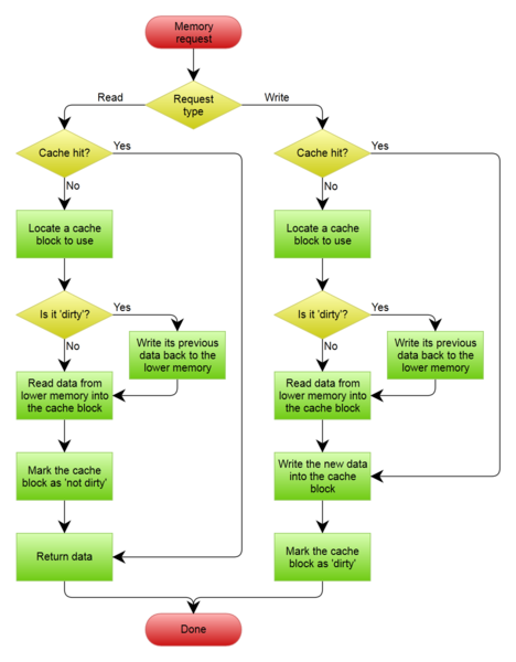
In a writeback, the cache is updated with a write but memory is not. Because of this, memory can contain stale values. When a block is being replace in the cache, the memory will be updated accordingly. This policy causes more stalls than write-through policy above. When an invalidation needs to occur, the memory might not have the most up to date values. Thus, a cache flush operation occurs in which every line in the cache is updated to memory. Writeback has more traffic during invalidation than write-through. Also, the processor whose cache has the latest value needs to be tracked. This is an additional overhead that write-through does not have.
Write Allocate/No Allocate, Fetch/No Fetch Policies
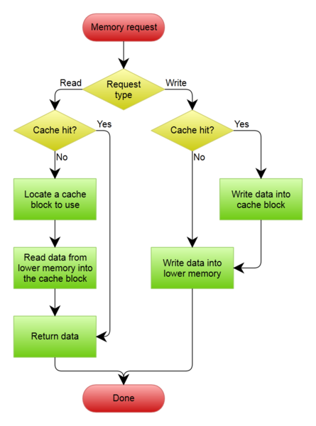
In Write Allocate policy, when a write misses, a line will be allocated in the cache for the data. In No-allocate, a line is not allocated as can be expected.
When a write allocate policy is used, the remaining data in line may be fetched employing the Fetch policy. In No-Fetch policy, the values in the line are not fetched from memory. In the fetch policy, all words in the line are valid and is simpler to execute than No-Fetch. In No-Fetch, all words in a line may not be valid and thus a valid bit is needed for each word.
Writeback caches tends to use Write-Allocate Fetch policy. Write-Through caches use No Allocate policy. The execution of these methods are shown in Figure 1.
Implementation with Write Buffer
Write-Through Cache<ref name="wrpol"/>
With a write-through cache, the write buffer will hold several lines to be updated into memory allowing the processor to continue without having to wait for the writes to complete.
There are two types of write buffer methods for the write-through cache.
- The write buffer can be a FIFO queue. When a write occurs, the write buffer will gather the address of the value of the write to be placed in an entry in the buffer. The writes will be updated to memory in FIFO order whenever the bus is available. The processor must stall when the buffer is full and another write is waiting to enter the buffer.
- Another method is for the write buffer to be a small write-back cache. It will act as a cache in that when a write occurs, it will check the address tag. If the tag matches, the data is put in that tag's line and a modified flag bit will be set high. If there is not tag match, a new line will be allocated or an old line will be replaced. The old line that is to be replaced will be updated to memory first. Memory will also be updated in the case of a buffer flush. This design is called writeback write buffer.
Writeback Write Buffer<ref name="wrpol"/>
The writeback write buffer actually reduces the stalls and traffic faced by a multiprocessors compared to a uniprocessor. The FIFO queue style write buffer has the same amount of write traffic as a uniprocessor and thus does not have control to prevent stalls in the case of memory being slow. Writeback write buffer is also easier to implement than the FIFO queue style.
The values in the writeback write buffer are updated to memory during a buffer flush. This is similar to how a writeback cache is flushed. However, the buffer flush does not create as much traffic due to the difference in size between the writeback write buffer and the writeback cache with the writeback write buffer being significantly smaller.
An issues with Write Buffers is when data trying to be read is in the write buffer and not in the cache. This is called a read conflict. This cannot be treated as a read miss, because the data in the memory has not yet been updated. Thus, another solution has to be implemented. One solution is to always check the write buffer before getting a value from memory when a read miss occurs. If the value is in the write buffer, then part or all of the write buffer will be flushed and the data required is fetched from memory. Another solution is to get the data from the write buffer but this would require a more complex design of the write buffer which has not been looked at here.
Writeback Cache
With a writeback cache, a line buffer is used as the write buffer. The line buffer will hold a single line to be updated into memory while a line is fetched from memory.
Comparing Different Cache-Buffering systems<ref name="wrpol"/>
Write-Through with No Buffering (WTNB): a write through cache with no-allocate policy with no write buffer
Write-Through with Buffering(WTB): a write-through cache with no-allocate policy with a FIFO queue write buffer

Write-Through with WriteBack Write Buffer(WTWB): a write through cache with no-allocate policy with a writeback write buffer
Write-Through Write-Allocate with Writeback Write Buffer(WTAWB): a write-through cache with write-allocate-no-fetch policy with the writeback write buffer
Writeback(WB): a writeback cache with write-allocate-fetch policy and a line write buffer
Information regarding the benchmarks used for comaprisons below are given in Table 1.
Hit Ratios

The cache hit ratio does not depend on whether the cache is write-through or write back. This is because these policies don't affect what data is in the cache, they affect when the data is written to memory. However, whether a cache is write-allocate or no-allocate affects the hit ratio.
Of the 5 configurations mentioned above, WTAWB and WB have a write-allocate policy. WTNB, WTB, and WTWB have a no-allocate policy. The use of a write-allocate policy increases the write and read hit ratios. The increase in write hit ratios benefits the writeback caches because it signifies it reduces the need to fetch data from memory because of misses. Increase in read hit benefits both writeback and write-through caches. It did not make a difference whether the caches used a fetch or no fetch policy. The fetch policy only makes a difference if a write miss is followed by a read to that same line. This does not occur often and thus did not make much of a difference. Table 2 shows the difference in hit ratios for write-allocate and no-allocate policies.
Memory Latency
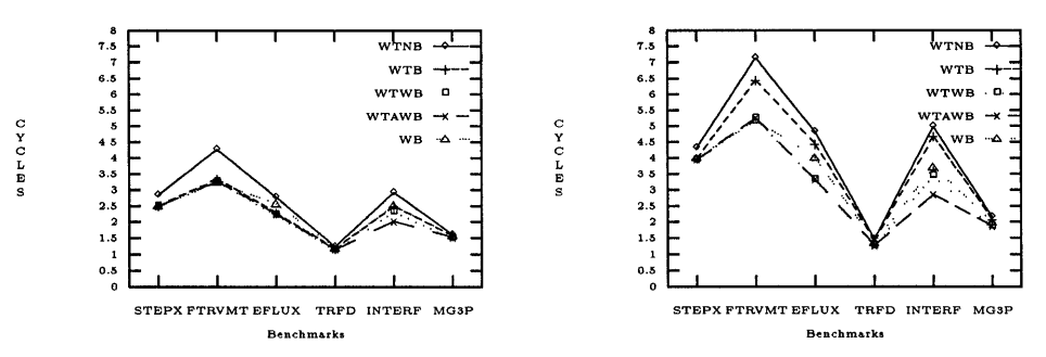
Hit ratios do not take into account write stalls and memory and network contention. This is reflected in average memory latency as it contains information about the time to access memory.
Fast Access System: WTNB has the highest memory latency for all the benchmarks. WTB, WTWB, WTAWB and WB perform similarly for four of the benchmarks. For EFLUX and INTERF benchmarks which have low write hit ratios, WB's latency increases. WTAWB has a lower latency for INTERF benchmark compared to WTWB and WTB because of its allocate policy. Thus WTAWB performs the best overall as shown in Figure 3.
Slow Access System: The results are similar for most configurations. However, WTB has a much higher latency now due to increase in stalls from the slow access system. Still, WTAWB outperforms the other configurations as shown again in Figure 3.

Execution Time
In parallelization, the instructions are split into epochs to allow synchronization between epochs. DOALL <ref>http://www-hydra.stanford.edu/publications/shspec.pdf</ref>loops are considered parallel epochs and serial code between DOALL loops are called sequential epochs as they have to be performed by one processor. After each epoch, a cache or buffer flush is required to update memory. A cache flush is required for writeback caches and a buffer flush is required for write-through caches with writebuffers.When a flush occurs, much of the content is invalid or has been unmodified. It takes various time to check/invalidate these lines causing differences in execution time.
Figure 4 shows execution times in relation to WTNB. Notice there is a WB(1) and WB here. WB(1) takes 1 cycle to check/invalidate a line while WB takes no time (or 0 cycles) to do so. WB and WB(1) have higher execution times because of the need for a cache flush. WTNB and WTB are slowed down for slow access systems because of an increased number of memory stalls. Again, WTAWB outperforms the other strategies because of not facing much degradation from a buffer flush due to its smaller buffer size.
Conclusion
The hit ratio comparison showed that write-allocate policy is better but it does not matter whether a fetch or no-fetch policy is implemented. WTAWB had the best performance for low memory latency and low execution times compared to the other configurations.
Sequential Coherency
Strong Ordering<ref name="ordering">http://www.ece.cmu.edu/~ece548/handouts/19coher.pdf</ref> In Strong Ordering, all memory accesses should be performed in program order and execute one at a time. This is the strictest of the ordering and thus does not allow much optimization.
Strongly-ordered models may be referred to as SC for sequential consistency.
SC are affected by the latency of store misses on the critical path (worst case) because loads must stall if there is an unresolved store miss. Increasing buffer size has no real effect because "few stores occur between consecutive loads." Prefetching and speculative stores can improve performance but store stalls still exist.
Total Store Ordering<ref name="ordering"/><ref name="storewaitfree"/> In total store ordering (TSO), stores must complete in order as opposed to all memory accesses. When a store miss occurs, all following stores are buffered. Stores in the buffer must commit in FIFO order.
Loads are allowed to bypass these stores. The critical time path in this case is the time it takes for loads to search through the buffer for its relevant store. TSO does require some synchronization to make sure that a processor can see if another processor has an updated value in its store buffer. If the store buffer gets full, it causes stalling and prevents further stores from retiring.
Partial Store Ordering<ref name="ordering"/> Partial Store Ordering is more relaxed than TSO. Here, stores to the same location must complete in order but stores to different locations can commit in any order.
Relaxed Memory Ordering<ref name="ordering"/><ref name="storewaitfree"/> A relaxed memory order (RMO) relaxes all order. This is also referred to as weak ordering. Stores in the store buffer may commit in any order. Because of the relaxation, RMO requires even more synchronization causing ordering delays.
Atomic Ordering<ref name="storewaitfree"/> A cause of a store delay is ordering constraints that stall the execution until in-flight stores have completed. Ordering stalls can be eliminated through atomic sequence ordering (ASO). Instead of enforcing ordering constraints on every memory access, it enforces ordering at a higher granularity. This access sequence will appear as an atomic sequence to other processors. A data race will expose an ordering violation and ASO will recover to the beginning of the nearest atomic sequence using a checkpoint-based rollback.
Atomic Ordering is examined in detail in the following section.
Atomic Sequence Ordering in Detail<ref name="storewaitfree">http://www.eecg.toronto.edu/~moshovos/research/store-wait-free.pdf</ref>
Function of ASO
ASO groups memory accesses into atomic sequences. As long as an atomic sequence appears atomic to other processors, the order of accesses in the sequence does not matter as it is not observable by other processors. An atomic sequence executes and either commits or is discarded because of a race condition. A data race exposes an ordering violation but is very rare. In this way, ASO eliminates unnecessary ordering stalls.
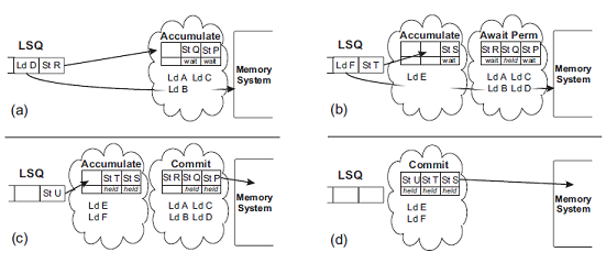
When an instruction would be stalled due to the ordering constraint, the system starts ASO. Figure 5 shows an example of ASO for two atomic sequences. An atomic sequence goes through 3 steps as shown in the diagram.
Step 1. A checkpoint is created when a new atomic sequence starts. At this point the atomic sequence is in an accumulate state. The memory accesses retire with speculative values ignoring ordering constraints. As this happens, the memory access instructions are added onto the atomic sequence. A write request is then sent for the cache blocks to be updated by the instructions in the sequence.
Step 2. Once an atomic sequence is of a certain predetermined size, a new checkpoint and atomic sequence are created. At this point, the old atomic sequence is in await permission state as it is waiting for all its write permissions.
Step 3. When an atomic sequence receives all its write permissions, it transitions into the commit state. At this point, it proceeds to update the memory system with its write values. All other processors writes are being stalled at this point to assume commit atomicity.
Step 4. A sequence can transition directly from accumulate to commit state if it already has its write permissions. This is shown by the second sequence in the figure.
Hardware Implementation
Tracking Atomic Sequences
As mentioned earlier, ASO is initialized once a instruction is not able to retire because of an out-standing store that is not yet complete. An Atomic Sequence Table (AST) will keep track of all the atomic sequences. For each atomic sequence, the AST will hold information about which instructions are in the sequence, a Lines counter to show which cache lines will be written to by the instructions in the sequence, and a Filled counter to show which write permissions have been obtained. When Filled equals Lines counter, it signifies that all the permissions for that sequence have arrived and the sequence may commit. In the L1 cache, each line has a SW (speculatively written) bit for each sequence in the AST. The bit indicates which atomic sequence's Filled counter to update when the line arrives. A new atomic sequence is created whenever the current sequences Lines count reaches a certain number, in this case, 16.
Detecting Atomicity Violations
To keep track of speculative reads in an atomic sequence, each line in the L1 and L2 cache is augmented with an SR (speculative read) bit for each sequence. If an invalidation matches a speculative line, then the atomic sequence must roll back accordingly. This must also occur if a line is evicted from L2 cache.
Committing Atomic Sequences
When a sequence has received all its permissions, it may commit values into the L2 cache. During this draining of instructions, other requests to access memory are stalled. SR and SW bits corresponding to the sequence are clears. It is easier to clear these bits if they are implemented using a specialized array rather than augmenting the existing caches. This causes very little storage overhead for the caches.
Rollback on Violation
To rollback in case of a violation, a checkpointing mechanism must be implemented. There must be one checkpoint for each atomic sequence present in the AST. A checkpoint must contain information regarding all register and the TLB/MMU (translation lookaside table/memory management unit) state. When a rollback occurs, all lines with a high SW bit are invalidated and the discarded sequences are removed from the AST.
Conclusion
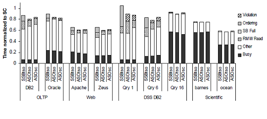
ASO removes ordering constraints and therefore reduces their penalties. Figure 6 shows the results of adding ASO to an execution with SSB. It has improved performance by 8%. In fact, ASO combined with scalable store buffer (SSB) outperforms even the RMO execution shown in Figure 8 in the Scalable Store Buffer section.
Write Buffer Implementations
Universal Read Write Buffer<ref name = "univrw">http://ieeexplore.ieee.org/xpls/abs_all.jsp?arnumber=342629&tag=1</ref>
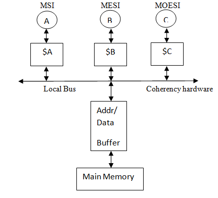
In multiprocessors with shared memory, if each processor has an individual write buffer to handle pending writes to the memory, it become complex to handle the memory operations in case of reads that require the data written by other processors. In such a case, the memory controller will have to incorporate snoopy mechanisms to figure which processor buffer has the latest data for the corresponding read address. To avoid these complications and to increase flexibility in design, the idea of a universal read/write buffer serves the purpose. It ensures that a FIFO order is maintained among the memory operations of all processors. The universal read/write buffer can also support multiprocessor cache coherence of different protocols. The interconnection network in shared memory multiprocessor systems leads to serialization of memory requests. It also needs to deal with communication contention to individual links in the network. Implementing various cache protocols such as the MSI, MESI & MOESI in multiprocessor systems allow coherency among the various caches and also help in reducing the bus traffic thereby improving performance of these systems.<ref>http://en.wikipedia.org/wiki/MOESI_protocol</ref> The various states are explained as follows:
M (Modified): valid, exclusive (does not exist in any other cache),dirty(meaning that the main memory does not hold a copy of the data)
S (Shared) : valid, copy can exist in other caches, clean (main memory has a copy of the data)
I (Invalid) : does not exist in memory or invalid copy of the data
E (Exclusive): valid, exclusive, clean
O (Owned) : valid, may be shared among caches, dirty, only one cache is in the owned state
In the universal read/write buffer mechanism explained in [CaoHuu,Yong,Lee]<ref name = "univrw"/>, the MSI and MESI protocols have been modified to further improve the performance of the system. As the MOESI protocol does not require write eviction to the memory in case of a read miss, i.e.it allows dirty sharing, the slow main memory accesses are less frequent in this coherence protocol. Hence the MSI and MESI protocols have been treated and monitored like the MOESI protocol.
The coherency hardware is depicted in Figure 7. $ implies a cache and $A implies private cache of processor A. The hardware includes the cache controller that is a finite state machine used to implement the various cache protocols.
Local Bus
The local bus monitors the status bits M,O,E,S,I , INTERVENE# and SHARE# bits to determine the current state and the next course of action that must follow. INTERVENE# bits are activated when there is a transfer of data from one cache to another SHARE#bits are activated by a cache controller if the new address is matched with any of its own tag ram address.
The local bus has three output signals that it provides to the buffer namely WB,LF and O3 each representing Write back cycle, line Feed cycle and Owned status bit. The WB signal is activated on two cases: when there is a read miss and the INTERVENE bits are asserted or when there is a write miss along with the M status
LF is activated on a read miss or a write miss from any protocol
O3 is connected to the MOESI cache controller and activated on a read miss and INTERVENE asserted. Mathematically, it can be represented as :
WB = RD * MOESI * INTV + WR * [STATUS=M]
LF = INTV
O3 = RD * MOESI * INTV
INTV implies INTERVENE
Assumptions in the approach : The Local Bus and Memory Bus have same bus width so that eviction and line-fill cycle need only one starting address.
All CPUs have same line size and memory controller can support that line size without interrupting. (one burst cycle for each line-fill and eviction cycle)
Address/Data Buffer
Functionally, the buffer consists of two parts, the data buffer and the address buffer.
- The Data Buffer consists of three FIFOs namely the Non_block Write FIFO, Write back FIFO and the read FIFO.
- The Address Buffer consists of a four deep FIFO for non-block write cycle, write-back FIFO for eviction cycle, line-fill FIFO for line fill cycle, snoop and byte gathering logic
Data Buffer The Non_block Write FIFO is used whenever there is a write to an address range non-specified in the memory map. This process does not require any block transfer (burst transfer) because there is no eviction or line-fill cycle. As a result, the Non_block Write FIFO provides a temporary storage area so that the CPU can start the next cycle immediately. The depth of the FIFO is arbitrary though more depth allows lower chances of the FIFO being full.
Write-back FIFO is used for eviction cycles. If there is a cache miss and eviction to main memory is required, the whole line of cache can be stored in burst mode (data transmitted in every clock). Right after this transaction, the new data can be read from main memory to cache (line-fill cycle) after which the data in write-back FIFO is written back to main memory. By doing so, the time required for writing-back a line of data will be hidden to CPU and new data will be available to CPU earlier. The depth of FIFO2 can be arbitrary.
The read FIFO is used for storing data from main memory or Posted-write/Write-back FIFO. When data from main memory or FIFOl or FIFO2 is ready but local bus is busy, the data will be temporarily stored in this FIFO until Local bus is cleared.
Latches and tri-state buffers hold data whenever memory bus (or local bus) is still busy and not ready for new data.
Address Buffer Non_block address FIFO for non-block write cycle, stores addresses for each non-block write cycle and provide them to main memory when system bus is available. The depth of the FIFO should be same as that of corresponding FIFO in the data buffer.
Write-back FIFO stores starting address of eviction cycle and provide the address to system bus when the bus is free. It is single level because memory controller can provide (or predict) next addresses within line boundary and the starting address of the line is the only necessary information for eviction cycle.
Line-fill FIFO, stores starting address of line-fill cycle and provide the address to system bus when the bus is free. It is single level because memory controller can provide (or predict) next addresses within line boundary and the starting address of the line is the only necessary information for line fill transfer
Whenever there is a read to a line that requires access to the main memory, the snoop logic is activated to compare the addresses in the WriteBack Address FIFO and the Line-fill Address FIFO to the read address. If any of the addresses matches, HIT flag is set and the data in the FIFO is read-back to Read FIFO through internal bypass path. By doing so, stale data will not be read and CPU doesn't have to waste lengthy memory latency time.
Snoop logic block also includes byte-gathering logic. Byte-gathering logic compares the incoming address and Byte-Enable (BE#) bits for non-block write cycle with that of previous non-block write cycle in non blocking address FIFO. If addresses are matched with no Byte-Enables overlapped, then the pointer of Non_block address FIFO will not advance. Therefore, the incoming data will stored in the same level of the Non_block address FIFO and prevents it from being filled up quickly.
Since read cycle has priority over write cycle, the read address will be provided directly to the memory bus whenever read cycle is issued and memory bus is available. In case memory bus is not free, the read address can be temporarily stored temporarily until bus becomes free.
Scalable Store Buffers<ref name="storewaitfree"/>
A store buffer is a storage containing retired store values prior to their release to memory. One cause of a store delay is insufficient store buffer capacity. A capacity stall is when a store instruction is not able to retire because all the store buffer entries are full. A scalable store buffer (SSB) helps eliminate these store buffer capacity stalls.
A store buffer capacity is “limited because every load must associatively search the buffer for a matching store, and this search is on the load’s critical path.” With SSB, there is no need for this associative search because speculative values are forwarded to loads straight from the L1 cache and committed values are maintained in the L2 cache. The SSB has stores in a FIFO order making it unnecessary to search through it associatively. However, it still allows an ordered commit to L2.
Functionality of SSB
In a conventional store buffer, the store buffer forwards values to the corresponding loads and it maintains the order among the stores. A load must search through the store buffer for a matching store. In contrast, an SSB forwards values to the loads through an L1 cache eliminating the need for this search. To be consistent in removing the need for this search, the stores in the SSB are in FIFO order which does not support an associative search. Stores commit in order from the SSB to L2 cache. Thus, L1 will contain speculative values and L2 will contain the committed values as mentioned above.
This allows the SSB capacity to equal L1’s capacity. This capacity is greater than that of a conventional store buffer. However, if an application requires a greater capacity, the SSB will be able to stall and wait for stores to drain just as a conventional store buffer does when its maximum capacity is reached.
Hardware Implementation
When a store retires, it updates the L1 cache and it is added to the SSB. There are valid bits added to each L1 line- one bit per word. These valid bits allow the data from L1 to be used in case of an out-standing store miss and allows merging with new data. The SSB contains the address, value and size of all stores in a FIFO structure (circular buffer). The size of the SSB is the same as the size of the L1 cache because there is no need for it to be associatively searched.
Invalidations
When two processors are trying to write to the same cache block at the same time, the cached block will be partially invalidated if the valid bit corresponding to that block is high. This means that the uncommitted stores in the SSB will be preserved while part of the global cache line in L2 will be invalidated. The valid bits in the line will be cleared and a request for write permission as well as the updated value is issued. When the updated line is received, the SSB "reconstructs the line by traversing the entire [SSB] to replay stores to the affected line, setting per-word valid bits as appropriate". This is an inefficient process but there is not much performance loss because invalidations tend to be very rare.
Sub-word writes
The design of the SSB is such that there is a valid bit for every word and not every byte. This means that writes of smaller than a word cannot take place unless all valid bits for that line are high/valid. In case of a sub-word miss, the sub-word is placed in a mini store buffer and waits until the line is filled. When multiple sub-word entries for the same word exist in the mini store buffer, an individual entry is created for the store in the SSB.
Conclusion
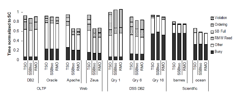
Conventional store buffers cannot eliminate store buffer capacity stalls. A SSB provides more capacity than is required by most application demands. Figure 8 shows the impacts of using an scalable store buffer.
There are three types of executions studied: SC, TSO, RMO. SC and RMO are two extremes. TSO is what is most applicable to our study. The figure shows that when we add a SSB to a TSO execution, all capacity stalls are eliminated and we get results similar to that of an RMO.
Partial Block Invalidation Coherence Mechanism<ref name="toussi"/>
Partially valid write-back mechanism
In this mechanism, a cache block is divided into two or more invalidation blocks each associated with its own valid bit. The individual valid bits are used to keep track of those invalidation blocks that have been modified. A dirty bit is also associated with the entire cache block. This bit implies that the block is exclusively stored in that particular cache block. A combination of the valid and dirty bits define the following three states of a cached block.
(a)Shared: Dirty reset + all valid bits set : Implies that cache block is valid and other copies may exist.A read leads to a cache hit.Write requires the invalidation of all the valid copies of the required invalidation block.It resets all the valid bits except that of the modified invalidation block.Dirty bit of the cache block is set.
(b)Owned: Dirty bit is set.The entire block is valid but copies of invalidation blocks may exist in other caches is the corresponding valid bit is not set.A read leads to a hit but a write requires invalidation of the block is the valid bit is reset.It sets the valid bit of the modified invalidation block.When an owned block is replaced,the contents must be written back to the main memory before reallocation.All valid bits must be checked for a hit or a miss.
(c)Stale: Dirty reset and atleast one valid bit is reset.Implies some other processor has written to the block.A write generates a write miss that causes the entire block to be written back to memory before the write miss is serviced.A read generates a miss only is the invalidation block is invalid.Otherwise,a hit is generated.
Partially valid write through mechanism
Each cache block is associated with a P-bit vector where P is the number of processors in the system to keep track of processors that contain a valid copy of the invalidation block.
The processors can be in the following two states:
(a) Shared : Same as the case of Write back caches except for a write reference also required forwarding the new data to the memory
(b) Invalid : Block is invalid in the cache as so the entire block must be fetched from the memory.A write miss causes invalidation of all other copies and a write through of new data to the main memory must be performed.A read or write miss sets the valid bits of all the invalidation blocks.
Write Buffers
The write through mechanism simplifies the process of detecting a hit by needing to check only one valid bit in the cache block. However,there is higher communication overhead due to writes to the main memory.In this case,a write buffer for the shared memory system can be used to reduce this communication overhead.The write buffer not only reduces the processor stalls on write misses by allowing multiple outstanding write requests, but also allows merging of writes to the same memory location till a synchronization point is reached instead of immediately forwarding the outstanding requests.The write buffer can be implemented as having one word per buffer entry or one block per buffer entry.Two words from the same block would occupy to position in the former configuration whereas one position in the latter configuration.The buffer is searched in a write operation to determine if there is already a block or word that has been previously written in order to merge the two changes.Otherwise,a new entry is allocated.In this mechanism,when the buffer is full,all the contents are flushed to the main memory and the processor is stalled during this operation. Both the write-through and the write-back caches allocate a block on a write miss and stall the processor on a read miss. If, on a read miss, the requested block is found in the write-buffer, the write-buffer is flushed back to memory. The read operation is performed after the buffer flushing is completed.
References
<references/>
See More
1.Consistency models : Shared Memory Consistency Models: A Tutorial http://www.hpl.hp.com/techreports/Compaq-DEC/WRL-95-7.pdf
2.Cache Write policies : http://www.hpl.hp.com/techreports/Compaq-DEC/WRL-91-12.html
3.Design Issues and tradeoffs of write buffers : ftp://128.112.136.55/pub/people/skadron/hpca3_wrt_buf.pdf
4.Multiprocessors and consistency models : http://research.cs.wisc.edu/multifacet/papers/computer98_sccase.pdf
5.Weak ordering : http://mprc.pku.cn/mentors/training/ISCAreading/1986/p434-dubois/p434-dubois.pdf
6.Cache coherence : https://parasol.tamu.edu/~rwerger/Courses/654/cachecoherence1.pdf
7.Fundamentals of Parallel Computer Architecture by Yan Sohilin Chapter 3:Shared memory parallel programming
8.Multiprocessor Cache Coherence: http://www.divms.uiowa.edu/~ghosh/4-20-06.pdf