CSC/ECE 506 Spring 2012/6b pa
Introduction
Ideally, in the case of write misses, the processor does not need to wait until the write is completed as it is not asking for any data.Hence,instead of stalling the processor,we can do the write action in the background,write the data into a write buffer and delegate the responsibility to the write buffer for performing the write to the memory hierarchy.Not stalling the processor under a write miss is good except when the write miss is followed by a read request to the same block and the write is pending in the write buffer.The solution to this problem lies in checking the write buffer for any pending writes to the requested block before requesting the data block from the next level of memory hierarchy.The following methods describe methods how to solve this issue when it comes to processors sharing a common memory in order to let other processors notice that the line is in fact in the write buffer and not in memory.
Universal Read/Write Buffers<ref>http://ieeexplore.ieee.org/xpls/abs_all.jsp?arnumber=342629&tag=1</ref>
Motivation
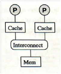
The uniform memory access class of MIMD(Multiple instruction Multiple data) parallel computers employ the Snoopy cache protocols (namely MSI,MESI and MOESI) mainly used to reduce bus traffic and to reduce the average memory access time for shared memory systems. Figure 1 depicts the shared memory system.

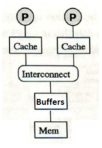
The main memory bandwidth of the shared memory systems is an important factor that affects the performance of the shared memory systems. This is because the off-chip bandwidth is low. A large number of writes to the main memory can lead to slower systems that need to wait for 100s of cycles until the slow main memory subsystem finishes the whole write access. Also, giving priority to reads over writes can improve the performance of the system as a whole. The universal read/write buffer supports multiprocessor cache coherence of the different cache coherence protocols in order to reduce the bandwidth of the memory bus to allow faster access than the main memory for both read and write accesses. It is located between the CPU’s local bus and the main memory. Figure 2 depicts the architecture of the universal read/write buffer scheme.

Hardware Description
Functionally, the buffer consists of two parts, the data buffer and the address buffer.
- The Data Buffer consists of three FIFOs namely the Non_block Write FIFO, Write back FIFO and the read FIFO.
- The Address Buffer consists of a four deep FIFO for non-block write cycle, write-back FIFO for eviction cycle, line-fill FIFO for line fill cycle, snoop and byte gathering logic
Data Buffer
The Non_block Write FIFO is a four deep FIFO used whenever there is a write to an address range non-specified in the memory map. This process does not require any block transfer (burst transfer) because there is no eviction or line-fill cycle. As a result, the Non_block Write FIFO provides a temporary storage area so that the CPU can start the next cycle immediately. The depth of the FIFO is arbitrary though more depth allows lower chances of the FIFO being full.
Write-back FIFO is eight-deep FIFO used for eviction cycles. If there is a cache miss and eviction to main memory is required, the whole line of cache can be stored in burst mode (data transmitted in every clock). Right after this transaction, the new data can be read from main memory to cache (line-fill cycle) after which the data in write-back FIFO is written back to main memory. By doing so, the time required for writing-back a line of data will be hidden to CPU and new data will be available to CPU earlier. The depth of FIFO2 can be arbitrary.
The Read FIFO is used for storing data from main memory or Posted-write/Write-back FIFO. When data from main memory or FIFOl or FIFO2 is ready but local bus is busy, the data will be temporarily stored in this FIFO until Local bus is cleared. MUX-A and MUX-B provide a data path between FIFOs and memory bus (or local bus). Latches and tri-state buffers hold data whenever memory bus (or local bus) is still busy and not ready for new data.
Address Buffer
The fourdeep FIFO for non-block write cycle, stores addresses for each non-block write cycle and provide them to main memory when system bus is available. The depth of the FIFO should be same as that of corresponding FIFO in data buffer.
Write-back FIFO stores starting address of eviction cycle and provide the address to system bus when the bus is free. It is single level because memory controller can provide (or predict) next addresses within line boundary and the starting address of the line is the only necessary information for eviction cycle.
Line-fill FIFO, stores starting address of line-fill cycle and provide the address to system bus when the bus is free. It is single level because memory controller can provide (or predict) next addresses within line boundary and the starting address of the line is the only necessary information for line fill transfer
Whenever there is a read to a line that requires access to the main memory, the snoop logic is activated to compare the addresses in the WriteBack Address FIFO and the Line-fill Address FIFO to the read address. If any of the addresses matches, HIT flag is set and the data in the FIFO is read-back to Read FIFO through internal bypass path. By doing so, stale data will not be read and CPU doesn't have to waste lengthy memory latency time.
Snoop logic block also includes byte-gathering logic. Byte-gathering logic compares the incoming address and Byte- Enable (BE#) bits for non-block write cycle with that of previous non-block write cycle in non blocking address FIFO. If addresses are matched with no Byte-Enables overlapped, then the pointer of FIFOl will not advance. Therefore, the incoming data will stored in the same level of FIFOl and prevents the FIFOl from being filled up quickly.
Since read cycle has priority over write cycle, the read address will be provided directly to the memory bus whenever read cycle is issued and memory bus is available. In case memory bus is not free, the read address can be temporarily stored in REG until bus becomes free.
Conclusion
The buffers function as a temporary storage for the written data so that lengthy main memory access time can be hidden. In this case,the CPU does not need to wait for the main memory cycle to finish then it can start another cycle. From the timing simulation results, it shows a 45% write cycle process improvement. In a normal write process, it takes 11 clock cycles to complete the entire write process. In other words, CPU is virtually busy in those 11 clock cycles. Hence, CPU can not proceed to another process until the write process is completed. It is, however, after adding the readwrite buffer, the originally required 11 clock cycles have been reduced to 6 cycles. Therefore, by using the read/write buffer, 5 cycles can be saved ( that means (1 14)/11 x 100% = 45% saving). This big saving definitely helps the overall system performance. This is because, for a CPU which occasionally writes to main memory, the read/write buffer can help saving thousands of clock cycles and free up the CPU much sooner. In fact, the performance is better than what it appears to be so far because the read buffer has not been taken into account in the above discussion. The read buffer helps to improve the performance even further. There are, without any doubts, many read processes from main memory to CPU during system operation. Hence, the read buffer help reducing the extra access time and meliorates the performance.
Scalable Store Buffers<ref>http://www.eecg.toronto.edu/~moshovos/research/store-wait-free.pdf</ref>
A store buffer is a storage containing retired store values prior to their release to memory. One cause of a store delay is insufficient store buffer capacity. A capacity stall is when a store instruction is not able to retire because all the store buffer entries are full. A scalable store buffer (SSB) helps eliminate these store buffer capacity stalls.
A store buffer capacity is “limited because every load must associatively search the buffer for a matching store, and this search is on the load’s critical path.” With SSB, there is no need for this associative search because speculative values are forwarded to loads straight from the L1 cache and committed values are maintained in the L2 cache. The SSB has stores in a FIFO order making it unnecessary to search through it associatively. However, it still allows an ordered commit to L2.
Functionality of SSB
In a conventional store buffer, the store buffer forwards values to the corresponding loads and it maintains the order among the stores. A load must search through the store buffer for a matching store. In contrast, an SSB forwards values to the loads through an L1 cache eliminating the need for this search. To be consistent in removing the need for this search, the stores in the SSB are in FIFO order which does not support an associative search. Stores commit in order from the SSB to L2 cache. Thus, L1 will contain speculative values and L2 will contain the committed values as mentioned above.
This allows the SSB capacity to equal L1’s capacity. This capacity is greater than that of a conventional store buffer. However, if an application requires a greater capacity, the SSB will be able to stall and wait for stores to drain just as a conventional store buffer does when its maximum capacity is reached.
Hardware Implementation
When a store retires, it updates the L1 cache and it is added to the SSB. There are valid bits added to each L1 line- one bit per word. These valid bits allow the data from L1 to be used in case of an out-standing store miss and allows merging with new data. The SSB contains the address, value and size of all stores in a FIFO structure (circular buffer). The size of the SSB is the same as the size of the L1 cache because there is no need for it to be associatively searched.
Invalidations
When two processors are trying to write to the same cache block at the same time, the cached block will be partially invalidated if the valid bit corresponding to that block is high. This means that the uncommitted stores in the SSB will be preserved while part of the global cache line in L2 will be invalidated. The valid bits in the line will be cleared and a request for write permission as well as the updated value is issued. When the updated line is received, the SSB "reconstructs the line by traversing the entire [SSB] to replay stores to the affected line, setting per-word valid bits as appropriate". This is an inefficient process but there is not much performance loss because invalidations tend to be very rare.
Sub-word writes
The design of the SSB is such that there is a valid bit for every word and not every byte. This means that writes of smaller than a word cannot take place unless all valid bits for that line are high/valid. In case of a sub-word miss, the sub-word is placed in a mini store buffer and waits until the line is filled. When multiple sub-word entries for the same word exist in the mini store buffer, an individual entry is created for the store in the SSB.
Conclusion
Atomic Sequence Ordering<ref>http://www.eecg.toronto.edu/~moshovos/research/store-wait-free.pdf</ref>
Function of ASO
Hardware Implementation
Conclusion
References
<references/>