CSC/ECE 506 Spring 2014/8a at: Difference between revisions
No edit summary |
No edit summary |
||
| Line 6: | Line 6: | ||
<br> | <br> | ||
<br> | <br> | ||
= Synapse Protocol = | |||
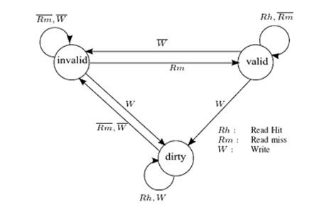
[[File:Synapse-sk.jpg|500px|thumbnail|State Transition Diagram for Synapse Protocol]] | |||
In Synapse protocol, cache blocks are in one of the following states: | |||
*'''Invalid''': Indicates that the block is invalid | |||
*'''Valid''': Indicates that the cache block is unmodified and possibly shared | |||
*'''Dirty''': indicates that the cache block is modified and there are no other copies. | |||
Only blocks in state Dirty are written back when replaced. Any cache with a copy of a block in state Dirty is called the owner of that block. If no Dirty copy exists, main memory is the owner.<br> | |||
==Implementation Complexities== | |||
The Synapse Expansion Bus includes an ownership level protocol between processor caches. It employs a non-write-through algorithm to minimize the bandwidth between cache and shared memory is employed in the cache to reduce memory contention. This protocol does not require a great deal of hardware complexity. Since an extra bit is added to the main memory to indicate whether a cache has an exclusive(Dirty) copy of the block, this needs to be implemented right to prevent malfunction of the protocol.<ref>[http://dl.acm.org/citation.cfm?id=1499317 Synapse tightly coupled multiprocessors: a new approach to solve old problems]</ref> | |||
<br> | |||
== Synapse N+1 multiprocessor== | |||
Synapse protocol was used in the [http://dl.acm.org/citation.cfm?id=327010.327222 Synapse N + 1], a multiprocessor for fault-tolerant transaction processing. The N + 1 differs from other shared bus designs considered in that it has two system buses. The added bandwidth of the extra bus allows the system to be expanded to a maximum of 28 processors. A single-bit tag is included with each cache block in main memory, indicating whether main memory is to respond to a miss on that block. If a cache has a modified copy of the block, the bit tells the memory that it need not respond. Thus if the bit is set, an access to the block fails until the data is written back to memory by the cache with the exclusive copy and the bit is reset. This prevents a possible race condition if a cache does not respond quickly enough to inhibit main memory from responding.<ref>[http://ctho.org/toread/forclass/18-742/3/p273-archibald.pdf Cache Coherence Protocols: Evaluation Using a Multiprocessor Simulation Model]</ref> | |||
<br><br> | |||
= MSI Protocol = | = MSI Protocol = | ||
[http://www.scribd.com/doc/50676653/19/MSI-protocol MSI] protocol is a three-state write-back invalidation protocol which is one of the simplest and earliest-used snooping-based cache coherence-protocols. | [http://www.scribd.com/doc/50676653/19/MSI-protocol MSI] protocol is a three-state write-back invalidation protocol which is one of the simplest and earliest-used snooping-based cache coherence-protocols. | ||
==Real Architectures using MSI== | ==Real Architectures using MSI== | ||
'''[http://en.wikipedia.org/wiki/MSI_protocol MSI]''' protocol was first used in '''[http://en.wikipedia.org/wiki/Silicon_Graphics SGI]''' IRIS 4D series. '''[http://en.wikipedia.org/wiki/Silicon_Graphics SGI]''' produced a broad range of '''[http://en.wikipedia.org/wiki/MIPS_architecture MIPS]'''-based (Microprocessor without Interlocked Pipeline Stages) workstations and servers during the 1990s, running '''[http://en.wikipedia.org/wiki/Silicon_Graphics SGI]''''s version of UNIX System V, now called '''[http://en.wikipedia.org/wiki/IRIX IRIX]'''. The 4D-MP graphics superworkstation brought 40 MIPS(million instructions per second) of computing performance to a graphics superworkstation | '''[http://en.wikipedia.org/wiki/MSI_protocol MSI]''' protocol was first used in '''[http://en.wikipedia.org/wiki/Silicon_Graphics SGI]''' IRIS 4D series. '''[http://en.wikipedia.org/wiki/Silicon_Graphics SGI]''' produced a broad range of '''[http://en.wikipedia.org/wiki/MIPS_architecture MIPS]'''-based (Microprocessor without Interlocked Pipeline Stages) workstations and servers during the 1990s, running '''[http://en.wikipedia.org/wiki/Silicon_Graphics SGI]''''s version of UNIX System V, now called '''[http://en.wikipedia.org/wiki/IRIX IRIX]'''. The 4D-MP graphics superworkstation brought 40 MIPS(million instructions per second) of computing performance to a graphics superworkstation. | ||
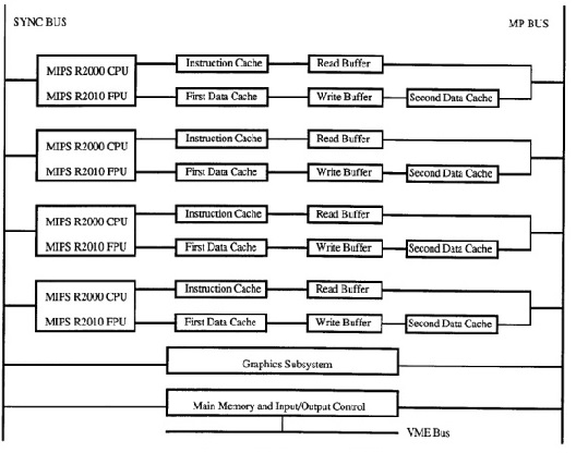
The multiprocessor bus used in 4D-MP graphics superworkstation is a pipelined, block transfer bus that supports the cache coherence protocol as well as providing 64 megabytes of sustained data bandwidth between the processors, the memory and I/O system, and the graphics subsystem | Such a high degree of computing and graphics processing was made possible by an intelligent Computing System Architecture as shown in Figure 1 below.(reference) The sync bus provides the required synchronization among the main processors(4 in this system) of the system. Processor buses provide full speed access to the L1 instruction and data caches. Each of the L1 caches are 64KB in size. Thus providing a 512 KB total cache size.The L2 Cache counts for another 512 KB memory of the system and is made up of four individual 64 KB caches. One important highlight of the 4D-MP is that the memory hierarchy is inclusive i.e., the L1 cache is a subset of the L2 cache. The multiprocessor(MP) bus used in 4D-MP graphics superworkstation is a pipelined, block transfer bus that supports the cache coherence protocol as well as providing 64 megabytes of sustained data bandwidth between the processors, the memory and I/O system, and the graphics subsystem. | ||
Every transaction on this MP bus is monitored by the L2 cache. The state for each cache line is maintained by it. It checks if the transactions involve data in its storage through a tag-matching mechanism and changes the state of the cache lines accordingly (States will be M/E/S/I depending on the requests). Write propagation is via the invalidation operation and Write serialization is via the MP bus. Consistency is guaranteed due to the Inclusion property of the Memory Hierarchy system. | |||
[[File:MSI.jpg]] | |||
==Implementation complexities== | ==Implementation complexities== | ||
| Line 185: | Line 187: | ||
<br/> | <br/> | ||
= References = | = References = | ||
<references/> | <references/> | ||
Revision as of 18:39, 22 March 2014
Introduction
Symmetric multiprocessing (SMP) involves a multiprocessor computer hardware architecture where two or more identical processors are connected to a single shared main memory via system bus. An SMP provides symmetric access to all of main memory from any processor and is the building block for larger parallel systems.
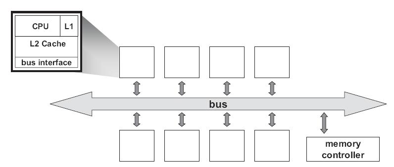
If each processor has a cache that reflects the state of various parts of memory, it is possible that two or more caches may have copies of the same line. It is also possible that a given line may contain more than one lockable data item. If two threads make appropriately serialized changes to those data items, the result could be that both caches end up with different, incorrect versions of the line of memory. In other words, the system's state is no longer coherent because the system contains two different versions of what is supposed to be the content of a specific area of memory. Various protocols have been devised to address the issue of cache coherence problem, such as MSI, MESI, MOESI, MERSI, MESIF, Synapse, Berkeley, Firefly and Dragon protocol. In this wiki article, MSI, MESI, MESIF, MOESI and Synapse protocol implementations on real architectures will be discussed.<ref>Cache Coherence</ref>
Synapse Protocol
In Synapse protocol, cache blocks are in one of the following states:
- Invalid: Indicates that the block is invalid
- Valid: Indicates that the cache block is unmodified and possibly shared
- Dirty: indicates that the cache block is modified and there are no other copies.
Only blocks in state Dirty are written back when replaced. Any cache with a copy of a block in state Dirty is called the owner of that block. If no Dirty copy exists, main memory is the owner.
Implementation Complexities
The Synapse Expansion Bus includes an ownership level protocol between processor caches. It employs a non-write-through algorithm to minimize the bandwidth between cache and shared memory is employed in the cache to reduce memory contention. This protocol does not require a great deal of hardware complexity. Since an extra bit is added to the main memory to indicate whether a cache has an exclusive(Dirty) copy of the block, this needs to be implemented right to prevent malfunction of the protocol.<ref>Synapse tightly coupled multiprocessors: a new approach to solve old problems</ref>
Synapse N+1 multiprocessor
Synapse protocol was used in the Synapse N + 1, a multiprocessor for fault-tolerant transaction processing. The N + 1 differs from other shared bus designs considered in that it has two system buses. The added bandwidth of the extra bus allows the system to be expanded to a maximum of 28 processors. A single-bit tag is included with each cache block in main memory, indicating whether main memory is to respond to a miss on that block. If a cache has a modified copy of the block, the bit tells the memory that it need not respond. Thus if the bit is set, an access to the block fails until the data is written back to memory by the cache with the exclusive copy and the bit is reset. This prevents a possible race condition if a cache does not respond quickly enough to inhibit main memory from responding.<ref>Cache Coherence Protocols: Evaluation Using a Multiprocessor Simulation Model</ref>
MSI Protocol
MSI protocol is a three-state write-back invalidation protocol which is one of the simplest and earliest-used snooping-based cache coherence-protocols.
Real Architectures using MSI
MSI protocol was first used in SGI IRIS 4D series. SGI produced a broad range of MIPS-based (Microprocessor without Interlocked Pipeline Stages) workstations and servers during the 1990s, running SGI's version of UNIX System V, now called IRIX. The 4D-MP graphics superworkstation brought 40 MIPS(million instructions per second) of computing performance to a graphics superworkstation.
Such a high degree of computing and graphics processing was made possible by an intelligent Computing System Architecture as shown in Figure 1 below.(reference) The sync bus provides the required synchronization among the main processors(4 in this system) of the system. Processor buses provide full speed access to the L1 instruction and data caches. Each of the L1 caches are 64KB in size. Thus providing a 512 KB total cache size.The L2 Cache counts for another 512 KB memory of the system and is made up of four individual 64 KB caches. One important highlight of the 4D-MP is that the memory hierarchy is inclusive i.e., the L1 cache is a subset of the L2 cache. The multiprocessor(MP) bus used in 4D-MP graphics superworkstation is a pipelined, block transfer bus that supports the cache coherence protocol as well as providing 64 megabytes of sustained data bandwidth between the processors, the memory and I/O system, and the graphics subsystem.
Every transaction on this MP bus is monitored by the L2 cache. The state for each cache line is maintained by it. It checks if the transactions involve data in its storage through a tag-matching mechanism and changes the state of the cache lines accordingly (States will be M/E/S/I depending on the requests). Write propagation is via the invalidation operation and Write serialization is via the MP bus. Consistency is guaranteed due to the Inclusion property of the Memory Hierarchy system.
Implementation complexities
In the MSI system, an explicit upgrade message is required for a read followed by a write, even if there are no other sharers. When a processor reads in and modifies a data item, two bus transactions are generated in this protocol even in the absence of sharers. The first is a BusRd that gets the memory block in S state, and the second is a BusRdX(or BusUpgr) that converts the blcok from S to M state. In this protocol, the complexity of the mechanism that determines the exclusiveness of the block is an aspect that needs attention. Also, in snoop-based cache-coherence protocols, the overall set of actions for memory operations is not atomic. This could lead to race conditions, and the issues of deadlock, serialization, etc. make it harder to implement.<ref>Snoop-based Multiprocessor Design</ref>
MESI Protocol
MESI protocol is a 4-state protocol, in which a cache block can have an 'Exclusive' state apart from the Modified, Shared and Invalid state as in MSI protocol.
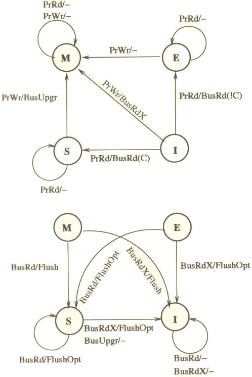
- Modified : The cache line contains valid data for an external memory location. However, the data does not match the data in the external since the processor has modiified the data since it was loaded from external memory. A cache that contains a modified line is responsible for ensuring that the data is properly maintained.
- Exclusive : The cache line contains valid data for some external memory location. The data exactly matches the data in the external memory location. Thus the cache block is clean, valid and exists only in one cache.
- Shared : The cache line conatins valid data for an external memory location, the data is shared by another cache, and the shared data matches the data in the external memory exactly; or the cache line is in write-through mode.
- Invalid : The cache line does not contain valid data for any external memory location. An invalid line does not participate in the cache coherence protocol.
The advantage of the MESI protocol over the MSI protocol lies in the fact that if the current cache has the Exclusive state, it can silently drop the cache block without issuing the expensive writeback operation. With the MESI protocol, the processor obtains the most current value everytime it is required.
In the MESI protocol, the same as the MSI protocol, processor requests to the
cache include:
- PrRd: processor-side request to read to a cache block
- PrWr: processor-side request to write to a cache block
Bus-side request, include:
- BusRd: snooped request that indicates there is a read request to a cache block made by another processor.
- BusRdX: snooped request that indicates there is a read exclusive (write)request to a cache block made by another processor which does not already have the block.
- BusUpgr: snooped request that indicates that there is a write request to a cache block that another processor already has in its cache.
- Flush: snooped request that indicates that an entire cache block is written back to the main memory by another processor.
- FlushOpt: snooped request that indicates that an entire cache block is posted on the bus in order to supply it to another processor. We distinguish FlushOpt from Flush because while Flush is needed for write propagation, FlushOpt is not required for correctness. It is implemented as a performance enhancing feature that can be removed without impacting correctness. It is referred to as an optional block flush cache-to-cache transfer.
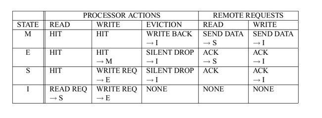
MESI states under different conditions is shown in the figure below:
CMP Implementation in Intel Architecture
Intel's Pentium Pro microprocessor, introduced in 1992, was the first Intel architecture microprocessor to support symmetric multiprocessing in various multiprocessor configurations. SMP and MESI protocol was the architecture used consistently until the introduction of the 45-nm Hi-k Core micro-architecture in Intel's (Nehalem-EP) quad-core x86-64. The 45-nm Hi-k Intel Core microarchitecture utilizes a new system of framework called the QuickPath Interconnect which uses point-to-point interconnection technology based on distributed shared memory architecture. It uses a modified version of MESI protocol called MESIF, which introduces the additional Forward state.<ref>CMP Implementation in Intel Core Duo Processors</ref> (The state diagram of MESI transitions that occur within the Pentium's data cache can be found on page 63 of Pentium Processor System Architecture: Second Edition by Don Anderson, Tom Shanley, MindShare, Inc)
CMP implementation on the Intel Pentium M processor contains a unified on-chip L1 cache with the processor, an Memory/L2 access control unit, a prefetch unit, and a Front Side Bus (FSB). Processor requests are first sought in the L2 cache. On a miss, they are forwarded to the main memory via FSB. The Memory/L2 access control unit serves as a central point for maintaining coherence within the core and with the external world. It contains a snoop control unit that receives snoop requests from the bus and performs the required operations on each cache (and internal buffers) in parallel. It also handles RFO requests (BusUpgr) and ensures the operation continues only after it guarantees that no other version on the cache line exists in any other cache in the system.<ref>CMP Implementation in Intel Core Duo Processors</ref> CMP implementation on the Intel Core Duo contains duplicated processors with on-chip L1 caches, L2 controller to handle all L2 cache requests and snoop requests, bus controller to handle data and I/O requests to and from the FSB, a prefetching unit, and a logical unit to maintain fairness between requests coming from each processors to L2 cache.
The Intel bus architecture has been evolving in order to accommodate the demands of scalability while using the same MESI protocol. From using a single shared bus to dual independent buses (DIB), doubling the available bandwidth, and to the logical conclusion of DIB with the introduction of dedicated high-speed interconnects (DHSI). The DHSI-based platforms use four FSBs, one for each processor in the platform. In both DIB and DHSI, the snoop filter was used in the chipset to cache snoop information, thereby significantly reducing the broadcasting needed for the snoop traffic on the buses. With the production of processors based on next generation 45-nm Hi-k Intel Core microarchitecture, the Intel Xeon processor fabric will transition from a DHSI, with the memory controller in the chipset, to a distributed shared memory architecture using Intel QuickPath Interconnects using MESIF protocol.
MESI in AMD's AM486DX microprocessors
AMD's enhanced Am486DX microprocessors implement the MESI protocol on systems with write-back cache support. These microprocessors allocate memory in the cache due to a read miss. Write allocation is not implemented.
To maintain coherence between cache and main memory, this protocol is implemented with the following characteristics:
- The system memory is always updated during a snoop when a modified line is hit.
- If a modified line is hit by another master during snooping, the master is forced off the bus and the snooped cache writes back the modified line to the system memory.
After the snooped cache completes the write, the forced-off bus master restarts the access and reads the modified data from memory.A cache line can occupy one of the four legal states M, E, S, I which can be indicated by the 2 bits in the tag entry.<ref>AMD-K6 -2E Embedded Processor Data Sheet Publication</ref>
ARM MPCore
The ARM11 MPCore and Cortex-A9 MPCore processors support the MESI cache coherency protocol.<ref>ARM</ref> ARM MPCore defines the states of the MESI protocol it implements as:
| Cache Line State: | Modified | Exclusive | Shared | Invalid |
| Copies in other caches | NO | NO | YES | - |
| Clean or Dirty | DIRTY | CLEAN | CLEAN | - |
The coherency protocol is implemented and managed by the Snoop Control Unit (SCU) in the ARM MPCore, which monitors the traffic between local L1 data caches and the next level of the memory hierarchy. At boot time, each core can choose to partake in the coherency domain or not. Unless explicit system calls bound a task to a specific core (processor affinity), there are high chances that a task will at some point migrate to a different core, along with its data as it is used. Migration of tasks is not efficiently implemented in literal MESI implementation, so the ARM MPCore offers two optimizations that allow for MESI compliance and migration of tasks: Direct Data Intervention (DDI) (in which the SCU keeps a copy of all cores caches’ tag RAMs. This enables it to efficiently detect if a cache line request by a core is in another core in the coherency domain before looking for it in the next level of the memory hierarchy)and Cache-to-cache Migration (where if the SCU finds that the cache line requested by one CPU present in another core, it will either copy it (if clean) or move it (if dirty) from the other CPU directly into the requesting one, without interacting with external memory). These optimizations reduce memory traffic in and out of the L1 cache subsystem by eliminating interaction with external memories, which in effect, reduces the overall load on the interconnect and the overall power consumption.<ref>ARM</ref>
Other architectures that use the MESI cache-coherence protocol include the L2 cache of the IBM POWER4 processor<ref>IBM POWER4</ref>, the L2 cache of the Intel Itanium 2 processor, and the Intel Xeon<ref>Intel Itanium 2</ref>.
Implementation Complexities
During replacement of a cache block, some MESI implementations require a message to be sent to memory when a cache line is flushed - an E to I transition, as the line was exclusively in one cache before it was removed. In alternate implementation, this replacement message could be avoided if the system is designed so that the flush of a modified /exclusive line requires an acknowledgment from the memory. However, this requires the flush to be stored in a 'write-back' buffer until the reply arrives to ensure the change is successfully propagated to memory.
According to the application, there is a bandwidth trade-off in both these applications. The MESI protocol has greater complexity in terms of block states and transitions. It requires a priority scheme for cache-to-cache transfers to determine which cache should supply the data when in shared state. In commercial implementations, usually the memory is allowed to update data. Like in the MSI protocol, this protocol too has the issues of complexity in issues of serialization, handshaking, deadlocks, etc. Also, the implementation of write-backs necessitates a write-buffer. The bus transactions relevant to buffered blocks must be handled carefully<ref>Discussion of cache coherence protocol implementation</ref>
MESIF Protocol
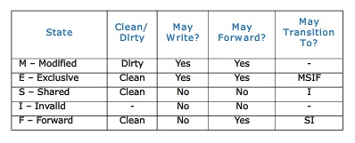
The MESIF protocol is a cache coherency and memory coherence protocol developed by Intel for cache coherent non-uniform memory architectures.The protocol consists of five states, Modified (M), Exclusive (E), Shared (S), Invalid (I) and Forward (F).
The M, E, S and I states are the same as in the MESI protocol. When a processor requests a cache line that is stored in multiple locations, every location might respond with the data. However, the requesting processor only needs a single copy of the data, so the system is wasting a bit of bandwidth. Intel's solution to this issue is rather elegant. They adapted the standard MESI protocol to include an additional state, the Forwarding (F) state, and changed the role of the Shared (S) state. In the MESIF protocol, only a single instance of a cache line may be in the F state and that instance is the only one that may be duplicated. Other caches may hold the data, but it will be in the shared state and cannot be copied. In other words, the cache line in the F state is used to respond to any read requests, while the S state cache lines are now silent. This makes the line in the F state a first amongst equals, when responding to snoop requests. By designating a single cache line to respond to requests, coherency traffic is substantially reduced when multiple copies of the data exist.
When a cache line in the F state is copied, the F state migrates to the newer copy, while the older one drops back to S. This has two advantages over pinning the F state to the original copy of the cache line. First, because the newest copy of the cache line is always in the F state, it is very unlikely that the line in the F state will be evicted from the caches. In essence, this takes advantage of the temporal locality of the request. The second advantage is that if a particular cache line is in high demand due to spatial locality, the bandwidth used to transmit that data will be spread across several nodes.
The table below summarizes the MESIF cache states:
MESIF in Intel Nehalem Computer
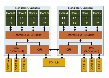
Intel Nehalem Computer uses the MESIF protocol. In the Nehalem architecture each core has its own L1 and L2 cache. Nehalem does has a shared cache, implemented as L3 cache. This cache is shared among all cores and is relatively large. This cache is inclusive, meaning that it duplicates all data stored in each indivitual L1 and L2 cache. This duplication greatly adds to the inter-core communication efficiency because any given core does not have to locate data in another processor’s cache. If the requested data is not found in any level of the core’s cache, it knows the data is also not present in any other core’s cache. To ensure coherency across all caches, the L3 cache has
additional flags that keep track of which core the data came from. If the data is modified in L3 cache, then the L3 cache knows if the data came from a different core than last time,and that the data in the first core needs its L1/L2 values updated with the new data. This greatly reduces the amount of traditional “snooping” coherency traffic between cores.<ref>Comparing Cache Organization and Memory Management of the Intel Nehalem Computer Architecture</ref>
The cache organization of a 8-core Intel Nehalem Processor is shown below:
MESIF in Intel® QuickPath Interconnect
The Intel QuickPath Interconnect is a high speed packetized point-to-point interconnect used in Intel's next generation of microprocessors introduced in second half of 2008. The narrow high speed links stitch together processors in distributed memory style platform architecture. The Intel QuickPath Interconnect includes the cache coherency protocol, MESIF to keep the distributed memory and shared caching coherent during system operation. It supports both low latency source snooping and direct cache-to-cache transfers for low latency.
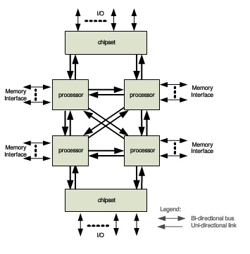
The Intel® QuickPath Interconnect coherency protocol consists of two distinct types of agents: caching agents and home agents. A micro-processor will typically have both types of agents and possibly multiple agents of each type. A caching agent represents an entity which may initiate transactions into coherent memory, and which may retain copies in its own cache structure. The caching agent is defined by the messages it may sink and source according to the behaviors defined in the cache coherence protocol. A caching agent can also provide copies of the coherent memory contents to other caching agents.A home agent represents an entity which services coherent transactions, including handshaking as necessary with caching agents. A home agent supervises a portion of the coherent memory. Home agent logic is not specifically the memory controller circuits for main memory, but rather the additional Intel® QuickPath Interconnect logic which maintains the coherency for a given address space. It is responsible for managing the conflicts that might arise among the different caching agents. It provides the appropriate data and ownership responses as required by a given transaction’s flow.
There are two basic types of snoop behaviors supported by the Intel® QuickPath Interconnect specification. Which snooping style is implemented is a processor architecture specific optimization decision. To over-simplify, source snoop offers the lowest latency for small multi-processor configurations. Home snooping offers optimization for the best performance in systems with a high number of agents.The home snoop coherency behavior defines the home agent as responsible for the snooping of other caching agents.The Intel® QuickPath Interconnect home snoop behavior implementation typically includes a directory structure to target the snoop to the specific caching agents that may have a copy of the data. This has the effect of reducing the number of snoops and snoop responses that the home agent has to deal with on the interconnect fabric. This is very useful in systems that have a large number of agents, although it comes at the expense of latency and complexity. Therefore, home snoop is targeted at systems optimized for a large number of agents.The source snoop coherency behavior streamlines the completion of a transaction by allowing the source of the request to issue both the request and any required snoop messages.The source snoop behavior offers lower latency at the expense of requiring agents to maintain a low latency path to receive and respond to snoop requests; it also imparts additional bandwidth stress on the interconnect fabric, relative to the home snoop method. Therefore, the source snoop behavior is most effective in platforms with only a few agents.<ref>The Common System Interface: Intel's Future Interconnect</ref>
Implementation Complexities
In comparision with the MESI protocol, the addition of 'Forward' state in the MESIF protocol reduces the complexity due to a reduction in the extent of communication between cores. This reduced communication is due to the design of specific state such that a single cache will respond to all the read requests for shared data. The implementation of write-backs necessitates a 'write-buffer' like in the case of MESI protocol, and the bus transactions relevant to these buffered blocks require careful handling. Though the inclusion of an additional state does increase design complexity, the working of this additional state and the concomitant decrease in communication between cores leads to the overall implementation complexity being similar to that in the MESI protocol.
MOESI Protocol
MOESI is a five state cache coherence protocol with the following states:
- Invalid: A cache line in the invalid state does not hold a valid copy of the data. Valid copies of the data can be either in main memory or another processor cache.
- Exclusive: A cache line in the exclusive state holds the most recent, correct copy of the data. The copy in main memory is also the most recent, correct copy of the data. No other processor holds a copy of the data.
- Shared: A cache line in the shared state holds the most recent, correct copy of the data. Other processors in the system may hold copies of the data in the shared state, as well. If no other processor holds it in the owned state, then the copy in main memory is also the most recent.
- Modified: A cache line in the modified state holds the most recent, correct copy of the data. The copy in main memory is stale (incorrect), and no other processor holds a copy.
- Owned: A cache line in the owned state holds the most recent, correct copy of the data. The owned state is similar to the shared state in that other processors can hold a copy of the most recent, correct data. Unlike the shared state, however, the copy in main memory can be stale (incorrect). Only one processor can hold the data in the owned state—all other processors must hold the data in the shared state.
MOESI is a more elaborate version of the simpler MESI protocol and avoids the need to write a dirty cache line back to main memory when another processor tries to read it. Instead, the Owned state allows a processor to supply the modified data directly to the other processor. This is beneficial when the communication latency and bandwidth between two CPUs is significantly better than to main memory. An example would be multi-core CPUs with per-core L2 caches. While MOESI can quickly share dirty cache lines from cache, it cannot quickly share clean lines from cache. If a cache line is clean with respect to memory and in the shared state, then any snoop request to that cache line will be filled from memory, rather than a cache. If a processor wishes to write to an Owned cache line, it must notify the other processors that are sharing that cache line. Depending on the implementation it may simply tell them to invalidate their copies (moving its own copy to the Modified state), or it may tell them to update their copies with the new contents (leaving its own copy in the Owned state).
MOESI in AMD64 architecture
The cache-coherency protocol supported by the AMD64 architecture is theMOESI. The figure beside shows the general MOESI state transitions possible with various types of memory accesses in AMD64 architecture. This is a logical software view, not a hardware view, of how cache-line state transitions. Instruction-execution activity and external-bus transactions can both be used to modify the cache MOESI state in multiprocessing or multi-mastering systems. To maintain memory coherency, external bus masters (typically other processors with their own internal caches) need to acquire the most recent copy of data before caching it internally. That copy can be in main memory or in the internal caches of other bus-mastering devices. When an external master has a cache read-miss or write-miss, it probes the other mastering devices to determine whether the most recent copy of data is held in any of their caches. If one of the other mastering devices holds the most recent copy, it provides it to the requesting device. Otherwise, the most recent copy is provided
by main memory.<ref>AMD 64 Technology</ref>
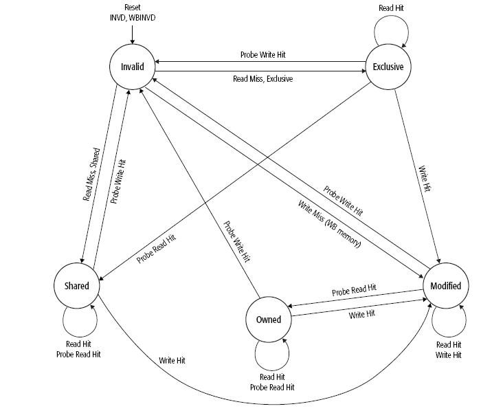
There are two general types of bus-master probes:
- Read probes indicate the external master is requesting the data for read purposes.
- Write probes indicate the external master is requesting the data for the purpose of modifying it.
The state transitions involving probes are initiated by other processors and external bus masters into the processor. Some read probes are initiated by devices that intend to cache the data. Others, such as those initiated by I/O devices, do not intend to cache the data.
Some processor implementations do not change the data MOESI state if the read probe is initiated by a
device that does not intend to cache the data.
State transitions involving read misses and write misses can cause the processor to generate probes into external bus masters and to read main memory. Read hits do not cause a MOESI-state change. Write hits generally cause a MOESI-state change into the modified state. If the cache line is already in the modified state, a write hit does not change its state. The specific operation of external-bus signals and transactions and how they influence a cache MOESI state are implementation dependent. For example, an implementation could convert a write miss to a WB memory type into two separate MOESI-state changes. The first would be a read-miss placing the cache line in the exclusive state. This would be followed by a write hit into the exclusive cache line, changing the cache-line state to modified.
Implementation Complexities
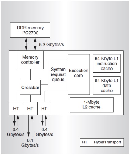
When implementing the MOESI protocol on a real architecture like AMD K10 series, some modification or optimization was made to the protocol which allowed more efficient operation for some specific program patterns. For example AMD Phenom family of microprocessors (Family 0×10) which is AMD’s first generation to incorporate 4 distinct cores on a single die, and the first to have a cache that all the cores share, uses the MOESI protocol with some optimization techniques incorporated.
It focuses on a small subset of compute problems which behave like Producer and Consumer programs. In such a computing problem, a thread of a program running on a single core produces data, which is consumed by a thread that is running on a separate core. With such programs, it is desirable to get the two distinct cores to communicate through the shared cache, to avoid round trips to/from main memory. The MOESI protocol that the AMD Phenom cache uses for cache coherence can also limit bandwidth. Hence by keeping the cache line in the ‘M’ state for such computing problems, we can achieve better performance.
When the producer thread , writes a new entry, it allocates cache-lines in the modified (M) state. Eventually, these M-marked cache lines will start to fill the L3 cache. When the consumer reads the cache line, the MOESI protocol changes the state of the cache line to owned (O) in the L3 cache and pulls down a shared (S) copy for its own use. Now, the producer thread circles the ring buffer to arrive back to the same cache line it had previously written. However, when the producer attempts to write new data to the owned (marked ‘O’) cache line, it finds that it cannot, since a cache line marked ‘O’ by the previous consumer read does not have sufficient permission for a write request (in the MOESI protocol). To maintain coherence, the memory controller must initiate probes in the other caches (to handle any other S copies that may exist). This will slow down the process.
Thus, it is preferable to keep the cache line in the ‘M’ state in the L3 cache. In such a situation, when the producer comes back around the ring buffer, it finds the previously written cache line still marked ‘M’, to which it is safe to write without coherence concerns. Thus better performance can be achieved by such optimization techniques to standard protocols when implemented in real machines.
You can find more information on how this is implemented and various other ways of optimizations in this manual Software Optimization guide for AMD 10h Processors
References
<references/>