CSC/ECE 506 Spring 2013/12b sl: Difference between revisions
No edit summary |
No edit summary |
||
| Line 149: | Line 149: | ||
==Ongoing Research in the area of On-Chip Optical Interconnects== | ==Ongoing Research in the area of On-Chip Optical Interconnects== | ||
On-chip optical interconnect has been considered as a potential substitute for electrical interconnect in the past two decades | On-chip optical interconnect has been considered as a potential substitute for electrical interconnect in the past two decades. The concept of on-chip optical interconnect was first introduced by Goodman in 1984. Since electrical/optical and optical/electrical conversion is required, optical interconnect is particularly attractive for global interconnects, such as data buses and | ||
clock distribution networks. | clock distribution networks. | ||
Recently, several comparisons have been made between on-chip electrical and optical interconnects. | Recently, several comparisons have been made between on-chip electrical and optical interconnects[http://www.csl.cornell.edu/~albonesi/research/papers/slip05.pdf]. | ||
==Optical On-chip Interconnects in recent times:== | ==Optical On-chip Interconnects in recent times:== | ||
Revision as of 23:25, 17 April 2013
On-chip interconnects
Introduction
The current trend in microprocessor design has shifted from extracting ever increasing performance gains from single core architecture to leveraging the power of multiple cores per die. This creates new challenges not present in single core systems. A multi core processor must have a method of passing information between processing cores that is efficient in terms of power consumed, space used on die, and the speed at which messages are delivered. As physical wire widths are decreased and the number of wires is increased, the difference between gate delay and wire delay is exacerbated.[14] To combat these challenges, much research has been done in the area of on-chip networks.
Background
On-chip interconnects are a natural extension of the high integration levels that nowadays are reached with multiprocessor integration. Moore's law predicted that the number of transistors in an integrated circuit doubles every two years. This assumption has driven the integration of on-chip components and continues to show the way in the semiconductor industry.
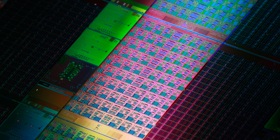
In recent years, the main players in the chip industry keep racing to provide more cores integrated in a chip, with the multi-core (more than one core) and many-core (multi-core with so many cores that the historical multi-core techniques are not efficient any longer) technologies. This integration is known as CMP (chip multiprocessor) and lately Intel has coined the term Intel® Many Integrated Core (Intel® MIC).
To make feasible the communication in between these many cores inside of a single chip, the traditional off-chip network has proved to have limited applications. According to [2], the off-chip designs suffered from I/O bottlenecks which are a diminished problem for on-chip technologies as the internal wiring provides much higher bandwidth and overcomes the delay associated with the external traffic. Nevertheless, the on-chip designs still have some challenges that need further study. Among some of these issues are power consumption and space constraints.
Terminology
Some common terms:
- SoCs (Systems-on-a-chip), which commonly refer to chips that are made for a specific application or domain area.
- MPSoCs (Multiprocessor systems-on-chip), referring to a SoC that uses multi-core technology.
It is interesting to note that for the particular theme of this article, there are at least three different acronyms referring to the same term. These are new technologies and different researchers have adopted different nomenclature. The acronyms are:
- NoC (network-on-chip), this is the most common term and also used in this article
- OCIN (on-chip interconnection network)
- OCN (on-chip network)
Topologies
Topology refers to the layout or arrangement of interconnections among the processing elements. In general, a good topology aims to minimize network latency and maximize throughput. There are certain metrics that help with the classification and comparison of the different topology types. Some of them are defined in Solihin's [3] textbook in chapter 12.
- Degree is defined as the number of nodes that are neighbors to, or in other words, can be reached from it in one hop
- Hop count is the number of nodes through which a message needs to go through to get to the destination
- Diameter is the maximum hop count
- Path diversity is useful for the routing algorithm and is given by the amount of shortest paths that a topology offers between two nodes.
- Bisection width is the smallest number of wires you have to cut to separate the network into two halves
Topologies can be classified as direct and indirect topologies.
In a direct topology, each node is connected to other nodes, which are named neighbouring nodes. Each node contains a network interface acting as a router in order to transfer information.
In an indirect topology, there are nodes that are no computational but act as switches to transfer the traffic among the rest of the nodes, including other switches. It is called indirect because packets are switched through specific elements that are not part of the computational nodes themselves.
An example of direct topologies is 2-D Mesh. An example of indirect topology is Flattened Butterfly.
There are many different topologies that could be introduced in this section. Some of the missing topologies include but are not limited to:
- Hypercube
- Shuffle-exchange
- Torus
- Trees
They are just cited here for completion, related information can be found at Interconnection Networks
Rings
Ring topologies can be effective when the “number of cores is still relatively small but is larger than what can be supported using a bus” [Solihin 409]. Such cases are considered to use “medium-scale” interconnection networks.
2-D Mesh
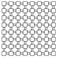
This has been a very popular topology due to its simple design and low layout and router complexity. It is often described as a k-ary n-cube , where k is the number of nodes on each dimension, and n is the number of dimensions. For example, a 4-ary 2-cube is a 4x4 2D mesh.
Another advantage is that this topology is similar to the physical die layout, making it more suitable to implement in tiled architectures. For reference, the combination of the switch and a processor is named tile.
But not everything are advantages in this topology. One of the drawbacks of 2D Meshes is that the degree of the nodes along the edges is lower than the degree of the central nodes. This makes the 2D Mesh asymmetrical along the edges, therefore from the networking perspective, there is less demand for edge channels than for central channels.
Jerger and Peh [2], provide the following information on parameters for a mesh as defined as a k-ary n-cube:
- the switch degree for a 2D mesh would be 4, as its network requires two channels in each dimension or 2n, although some ports on the edge will be unused.
- average minimum hop count:
nk/3 k even n(k/3-1/3k) k odd
- the channel load across the bisection of a mesh under uniform random traffic with an even k is k/4
- meshes provide diversity of paths for routing messages
Concentration Mesh
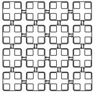
This is an evolution of the mesh topology. There is no real need to have a 1:1 relationship between the number of cores and the number of switches/routers. The Concentration mesh reduces the ratio to 1:4, i.e. each router serves four computing nodes.
The advantage over the simple mesh is the decrease in the average hop count. This is important in terms of scaling the solution. But it is not as scalable as it could seem, as its degree is confined to the crossbar complexity [1]
The reduction in the ratio introduces a lower bisection channel count, but it can be avoided by introducing express channels, as demonstrated in [4].
Another drawback is that the port bandwidth can become a bottleneck in periods of high traffic.
Flattened Butterfly
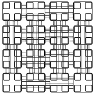
A butterfly topology is often described as a k-ary n-fly, which implies kn network nodes with n stages of kn−1 k × k intermediate routing nodes. The degree of each intermediate router is 2k.
The flattened butterfly is made by flattening (i.e. combining) the routers in each row of a butterfly topology while preserving the inter-router connections. It does non-minimal routing for load balancing improvement in the network. Some advantages are that the maximum distance between nodes is two hops and it has lower latency and better throughput than that of the mesh topology. For the disadvantages, it has high channel count (k2/2 per row/column), low channel utilization, and increased control complexity. The flattened butterfly offers the benefits of a tree (less constraints on root-level bandwidth [Solihin 367]) as well as the ability to actually be mapped to a substrate, but because of node concentration<ref name="GrotKeckler"/> the number of channels required for high scalability is cost- and validation-prohibitive.
Crossbar Switch
A crossbar switch topology uses a bus arrangement with the bus lines physically perpendicular to each other and whose intersections are connected or disconnected with a switch. In the case of CMPs, this switch is a transistor or, depending on the desired characteristics of the system, a programmable fuse. Due to their ability to be multi-staged<ref name="wikicrossbarsemi">"Crossbar switch." Wikipedia. Last accessed April 24, 2012.</ref>, these topologies lend themselves to being used for memory in large-scale systems. The IBM Cyclops64 architecture is an example of the implementation of this architecture<ref name="cyclops64">Zhang, Ying Ping. "A study of the on-chip interconnection network for the IBM Cyclops64 multi-core architecture. April 2006. IEEE Xplore.</ref>.
Multidrop Express Channels (MECS)
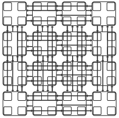
Multidrop Express Channels was proposed in [1] by Grot and Keckler. Their motivation was that performance and scalability should be obtained by managing wiring.
Multidrop Express Channels is defined by its authors as a "one to-many communication fabric that enables a high degree of connectivity in a bandwidth-efficient manner." Based on point-to-point unidirectional links. This makes for a high degree of connectivity with fewer bisection channels and higher bandwidth for each channel.
Some of the parameters calculated for MECS are:
- Bisection channel count per each row/column is equal to k.
- Network diameter (maximum hop count) is two.
- The number of nodes accessible through each channel ranges from 1 to k − 1.
- A node has 1 output port per direction
- The input port count is 2(k − 1)
The low channel count and the high degree of connectivity provided by each channel increase per channel bandwidth and wire utilization. At the same time, the design minimizes the serialization delay. It presents low network latencies due to its low diameter.
Comparison of topologies
This data is taken from the analysis done in [1].

The information in this table compares three of the topologies described above for two combinations of k which is the network radix (nodes/dimension) and c (concentration factor, 1 being no concentration).
Maximum hop count is 2 for flattened butterfly and MECS, whereas is directly proportional to k in the case of Concentrated Mesh, what makes flattened butterfly and MECS better solutions with less network latency.
The bisection channels is 1 for CMesh in both cases, but it gets doubled and even quadrupled between MECS and flattened butterfly.
The bandwidth per channel in this example is better for CMesh and MECS, getting attenuated in the case of flattened butterfly.
Examples of topologies in current NoCs and on-going research by different vendors
Intel
The Intel Teraflops Research Chip is made of an 8x10 mesh, and two 38-bit unidirectional links per channel. It has a bisection bandwidth of 380 GB/s, this includes data and sideband communication. There is a 5-port router inside of each of the computing nodes and the communication is carried out through message-passing. Its name comes from the one trillion mathematical calculations per second (1 Teraflops) of performance, accomplished with the 80 simple cores with each containing 2 floating point units and all of this consuming only 62 watts (less than many other processors).
The Single-Chip Cloud Computer contains a 24-router mesh network with 256 GB/s bisection bandwidth. This design contains 48 fully functional cores and consumes only 25 watts. This newer model is more complete than the Teraflops Research model. It is full programmable and used for research by academia and private companies.
Tilera
Tilera Tilera TileGx, TilePro, and Tile64 is a fabless semiconductor company that has developed a "tile processor" whereby the fabrication of the multi-processor device is greatly simplified by the placement of processor "tiles" on the die. The technology behind this innovation is iMesh, which is the name of the on-chip interconnection technology used in the Tile Processor's architecture<ref name="Tilera">"On-Chip Interconnection Architecture of the Tile Processor," Wentzlaff, et al. 2007. IEEE Xplore.</ref>. The iMesh™ consists of five 8x8 independent mesh networks with two 32-bit unidirectional links per channel. The Tile Processor is innovative due to its highly scalable implementation of an on-chip network that utilizes 2D meshes. These are physically organized (as opposed to logically organized) due to design considerations when scaling and laying out new designs.It provides a bisection bandwidth of 320GB/s. The tiles that conform the Tilera designs contain a complete processor with L1 and L2 caches. And each one can run an operating system in an independent manner or several tiles can run, together as a whole, an operating system like SMP Linux, for example.
ST Microelectronics
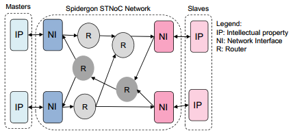
ST Microelectronics created the Spidergon design for the STNoC [5].
The Spidergon is a pseudo-regular topology with a design that is composed of three building blocks: network interface, router, and physical link. These building blocks make the design ready to be tailored to the needs of the application. Each router building block has a degree of 3.
The 3 building blocks can be used to create the specific design needed, with the input/output ports that the application requires. The blocks can be configured and stored in a library for creating the design. In the picture on the right, the example contains 2 of the building blocks (router and network interface) and a third undisclosed block.
IBM
The IBM Cell project uses an interconnect with four unidirectional 16B-wide data rings, two in each direction. The name of the interconnect is the Element Interconnect Bus (EIB) and allows for communication among the different components of the Cell, among them and with the external I/O. The total network bisection bandwidth is 307.2 GB/s.
As a curiosity, the Cell processor was jointly developed with Sony and Toshiba, and is used in the Sony PlayStation 3. The Cell consists of a PowerPC core which manages eight synergistic processing engines (SPEs) that can be used for floating-point calculations. These calculations provide the engine for better gaming systems.
IBM Cyclops-64 (C64) - St is a petaflop supercomputer built on multi-core system-on-a-chip technology. Each C64 chip employs a multistage pipelined crossbar switch as its on-chip interconnection network to provide high bandwidth and low latency communication between the 160 thread processing cores, the on-chip SRAM memory banks, and other components.
The C64 crossbar is a stable network and has the potential to reach the full hardware bandwidth and exhibit a non-blocking behavior. The network logic design appears to provide a reasonable opportunity for sharing the channel bandwidth between traffic in either direction.
ARM CoreLink Interconnect
The ARM CoreLink Interconnect is a highly flexible and configurable interconnection network specification that implements the AMBA (Advanced Microcontroller Bus Architecture) protocol. The AMBA protocol is "an open standard, on-chip interconnect specification for the connection and management of functional blocks in a System-on-Chip (SoC). It enables development of multi-processor designs with large numbers of controllers and peripherals."<ref name="ambadoc">AMBA on the ARM Info Center.</ref>
Ongoing Research in the area of On-Chip Optical Interconnects
On-chip optical interconnect has been considered as a potential substitute for electrical interconnect in the past two decades. The concept of on-chip optical interconnect was first introduced by Goodman in 1984. Since electrical/optical and optical/electrical conversion is required, optical interconnect is particularly attractive for global interconnects, such as data buses and clock distribution networks. Recently, several comparisons have been made between on-chip electrical and optical interconnects[1].
Optical On-chip Interconnects in recent times:
On December 10, 2012 IBM announced a breakthrough optical communication technology which has been verified in a manufacturing environment. The technology – called “silicon nanophotonics” – uses light instead of electrical signals to transfer information for future computing systems, thus allowing large volumes of data to be moved fast between computer chips in servers, large data-centers, and supercomputers via pulses of light.
Routing
There are a variety of routing protocols that can be used for SoC's, each having different advantages and disadvantages. They can be broadly classified in several different ways.
General Routing Schemes
Store and forward routing
This routing scheme has been used since the early days of telecommunications. It requires that the entire message be received at a node prior before it is propagated to the next node. This protocol suffers from a high storage requirement and high latency, due to the need to completely buffer a message before forwarding it.[7] This approach can be quite effective when the average packet size is small in comparison with the channel widths.
Cut-Through routing or Worm Hole routing
These two protocols uses the switch to examine the flit header, decide where to send the message, and then start forwarding it immediately. True cut-through routing lets the tail continue when the head is blocked, stacking message packets into a single switch (which requires a buffer large enough to hold the largest packet). In worm hole routing, when the head of the message is blocked the message stays strung out over multiple nodes in the network, potentially blocking other messages (however, this needs only enough buffer space to store the piece of the packet that is sent between switches). Using a cut-through protocol lowers latency but can suffer from packet corruption and must implement a scheme to handle this.[7]
Deterministic routing
This describes a routing scheme where, if we are given a pair of nodes, the same path will always be used between those nodes.
Adaptive routing
This is a routing scheme where the underlying routers may alter the path of packet flow in response to system conditions or other algorithm criteria. Adaptive routing is intended to provide as many routes as possible to reach the destination.
Deadlock and Livelock
Deadlock and livelock are two separate situations that may occur during routing, both resulting in packets never reaching their destination. They are defined as follows:
Deadlock is defined as a situation where there are activities (e.g., messages) each waiting for another to finish something.[8] Since a waiting activity cannot finish, the messages are deadlocked. This is analogous to the Dining Philosophers Problem, each deadlocked message is waiting on the result of another deadlocked message, and none are able to reach their destination.
Livelock is defined as a situation where a message can move from node to node but will never reach their destination node.[8] This is similar to deadlock in that the message never reaches its destination, but the message is still able to travel through portions of the network, making hops but never reaching its target. This is analogous to a process spinning while waiting, the process itself is doing meaningless work but it is still active.
Routing Protocols in SoC's
The specific routing protocols below are built using the ideas from the classes of protocols previously described.
Source Routing
The source node partially or totally computes the path a packet will take through the network and stores the information in the packet header. The extra route information is sent in each packet, inflating their size.
Distributed Routing
Each switch in the network computes the next route that will be taking towards the destination. The packet header contains only the destination information, reducing its size compared to source routing. This approach requires routing tables to be present to direct the packet from node to node, which does not scale well when the number of nodes increases.
Logic Based Distributed Routing (LBDR)
In this protocol, routing is achieved by each router knowing its position in the architecture and being able to determine what direction it is from the destination of the packet. It is most commonly used in 2D meshes, but it can be applied to other topologies as well.[7] Using this position information, it is possible to route the packet based on a small number of bits and a few logic gates per router, which saves over a table or a buffer.
There are several variations of LBDR
LBDRe - This variation models up to two future hops before deciding where to send the packet next.
uLBDR (Universal LBDR) - This variation adds packet multicast support to the protocol.
bLBDR - This variation adds the ability to broadcast messages to only certain regions (segments) of the network.
Bufferless Deflection Routing (BLESS protocol)
In this protocol, each flit of a packet is routed independently of every other flit through the network, and different flits from the same packet may take different paths. Any contention between multiple flits results in one flit taking the desired path and the other flit being “deflected” to some other router. This may result in undesirable routing, but the packets will eventually reach the destination.[10] This type of routing is feasible on every network topology that satisfies the following two constraints: Every router has at least the same number of output ports as the number of its input ports, and every router is reachable from every other router.[10]
CHIPPER (Cheap-Interconnect Partially Permuting Router)
This protocol was designed to address inefficient port allocation in the BLESS protocol. A permutation network directs deflected flits to free output ports. By limiting the requirements so that only that the highest-priority flit obtains its request, we can prevent livelock. In the case of contention, arbitration logic chooses a winning flit. It does this by choosing a single packet, and prioritize that packet globally above all other packets for long enough that its delivery is ensured. Every packet in the system eventually receives this special status, so every packet is eventually delivered (the Golden Packet scheme).[11]
Dimension-order Routing
This protocol is a deterministic strategy for multidimensional networks. Each direction is chosen in order and routed completely before switching to the next direction. For example, in a 2D mesh, dimension order routing could be implemented by completely routing the packet in the X-dimension before beginning to route in the Y-dimension. This is extensible to higher order connections as well, for example, hypercubes can be routed in dimension order by routing packets along the dimensions in the order of different bit positions of the source and destination address, one bit position at a time.[9]
Lines of Research
From NoCs perspective, there are many lines of research besides the abundant of technologies of the commercial designs. Some of them are presented in this section.
Optical on-chip interconnects
IBM has been performing extensive research on photonic layer inside of the CMP used not only for connecting several cores, but also for routing traffic: Silicon Integrated Nanophotonics. This technology was actually used in the IBM Cell chip that was mentioned in above sections. The main advantages are reliability and power efficiency.
This tutorial explains some differences between electronics and photonics in terms of power consumption, the more efficient is the computing from power's perspective, the more FLOPs per Watt:
| Electronics | Photonics |
| Electronic network ~500W | Optic network <80W |
| power = bandwidth x length | power does not depend on bitrate nor length |
| buffer on chip that rx and re-tx every bit at every switch | rx (modulate) data once, without having to re-tx |
| switching fabric has almost no power dissipation |
In academia, there are articles like [6] which proposes a new topology created for optical on-chip interconnects. They refer to previous papers that cite adaptations of well-known electronic designs, but highlight the need to provide a "scalable all-optical NoC, referred to as 2D-HERT, with passive routing of optical data streams based on their wavelengths."
Reconfigurable NoC
Another field of study is the Software reconfigurable on-chip networks. They are commonly based on the 2D mesh topology. The main idea is to be able to reconfigure the NoC depending on the application and during run-time to react to congestion problems or, in general, adapt to the traffic load.
In [12], the authors propose a design based on the properties of the field-programmable gate array (FPGA). It can dynamically implement circuit-switching channels, perform variations in the topology, and reconfigure routing tables. One of the main drawbacks is the overhead that this reconfiguration introduces, although it is designed to minimize it.
Bio NoC
Bio NoC or ANoC (Autonomic Network-on-Chip) is based on the concept of the human autonomic nervous system or the human biological immune system. The intention is to provide a NoC with self-organization, self-configuration, and self-healing to dynamically control networking functions.
[13] presents a collection of chapters/articles from emerging research issues in the ANoC field of application.
See also
[1] Mirza-Aghatabar, M.; Koohi, S.; Hessabi, S.; Pedram, M.; , "An Empirical Investigation of Mesh and Torus NoC Topologies Under Different Routing Algorithms and Traffic Models," Digital System Design Architectures, Methods and Tools, 2007. DSD 2007. 10th Euromicro Conference on , vol., no., pp.19-26, 29-31 Aug. 2007
[2] Ying Ping Zhang; Taikyeong Jeong; Fei Chen; Haiping Wu; Nitzsche, R.; Gao, G.R.; , "A study of the on-chip interconnection network for the IBM Cyclops64 multi-core architecture," Parallel and Distributed Processing Symposium, 2006. IPDPS 2006. 20th International , vol., no., pp. 10 pp., 25-29 April 2006
[3] David Wentzlaff, Patrick Griffin, Henry Hoffmann, Liewei Bao, Bruce Edwards, Carl Ramey, Matthew Mattina, Chyi-Chang Miao, John F. Brown III, and Anant Agarwal. 2007. On-Chip Interconnection Architecture of the Tile Processor. IEEE Micro 27, 5 (September 2007), 15-31.
[4] D. N. Jayasimha, B. Zafar, Y. Hoskote. On-chip interconnection networks: why they are different and how to compare them. Technical Report, Intel Corp, 2006
[5] John Kim, James Balfour, and William Dally. Flattened butterfly topology for on-chip networks. In Proceedings of the 40th International Symposium on Microarchitecture, pages 172–182, December 2007.
References
[1] B. Grot and S. W. Keckler. Scalable on-chip interconnect topologies. 2nd Workshop on Chip Multiprocessor Memory Systems and Interconnects, 2008.
[2] Natalie Enright Jerger and Li-Shiuan Peh. On-Chip Networks. Synthesis Lectures on Computer Architecture. 2009, 141 pages. Morgan and Claypool Publishers.
[3] Yan Solihin. (2008). Fundamentals of parallel computer architecture. Solihin Pub.
[4] James Balfour and William J. Dally. 2006. Design tradeoffs for tiled CMP on-chip networks. In Proceedings of the 20th annual international conference on Supercomputing (ICS '06). ACM, New York, NY, USA, 187-198.
[5] Dubois, F.; Cano, J.; Coppola, M.; Flich, J.; Petrot, F.; , Spidergon STNoC design flow, Networks on Chip (NoCS), 2011 Fifth IEEE/ACM International Symposium on , vol., no., pp.267-268, 1-4 May 2011
[6] Koohi, S.; Abdollahi, M.; Hessabi, S.; , All-optical wavelength-routed NoC based on a novel hierarchical topology, Networks on Chip (NoCS), 2011 Fifth IEEE/ACM International Symposium on , vol., no., pp.97-104, 1-4 May 2011
[7] Flich, J.; Duato, J.;, Logic-Based Distributed Routing for NoCs, 2008 Computer Architecture Letters, vol. 7, no. 1, pp.13-16, Jan 2008
[8] Wu, J.; A Fault-Tolerant and Deadlock-Free Routing Protocol in 2D Meshes Based on Odd-Even Turn Model, 2003 IEEE Transactions on Computers, Vol. 52, No. 9, pp.1154-1169, Sept 2003
[9] Veselovsky, G.; Batovski, D.A.; A study of the permutation capability of a binary hypercube under deterministic dimension-order routing, 2003 Parallel, Distributed and Network-Based Processing, 2003. Proceedings. Eleventh Euromicro Conference on, vol., no., pp.173-177, 5-7 Feb. 2003
[10] Moscibroda, T; Mutlu, O.; A Case for Bufferless Routing in On-Chip Networks, ACM SIGARCH Computer Architecture News, Volume 37 Issue 3, June 2009
[11] Fallin, C.; Craik, C.; Mutlu, O.; CHIPPER: A Low-complexity Bufferless Deflection Router, Proceedings of the 17th IEEE International Symposium on High Performance Computer Architecture (HPCA 2011), San Antonio, TX, February 2011.
[12] V. Rana, et al., A Reconfigurable Network-on-Chip Architecture for Optimal Multi-Processor SoC Communication, in VLSI-SoC, 2009.
[13] Cong-Vinh, P. (December 2011). Autonomic networking-on-chip: Bio-inspired specification, development, and verification. CRC Press.
[14] S. Kumar, et al., A Network on Chip Architecture and Design Methodology, VLSI on Annual Symposium, IEEE Computer Society ISVLSI 2002.
Quiz
1. Advantage of 2-D Mesh
a) simple design
b) cumbersome design
c) degree is the same for all nodes
2. Diameter is
a) minimum hop count
b) maximum hop count
c) number of neighbors
3. SOC stands for
a) System of Chips
b) Switch of Cores
c) System on a Chip
4. In a direct topology,
a) each node contains a network interface acting as a router in order to transfer information
b) there are nodes that act as routers
c) only one node is a computational nodes
5. The Single-Chip Cloud Computer contains
a) an 8x10 mesh
b) a 64-router mesh network
c) a 24-router mesh network
6. A deterministic routing scheme uses algorithms to determine the most advantageous path to the target node.
a) True
b) False
7. Livelock is necessary to maintain coherence in routing protocols.
a) True
b) False
8. Dimension Order routing
a) is only possible with 2D mesh-based topologies.
b) attempts to route all packets in one dimension before starting another.
c) uses routing tables to find the packet destination.
9. Source routing
a) includes information in the packet about the destination node
b) uses routing information calculated by the sending node
c) all of the above
10. Store and forward routing
a) requires the entire message to be broken into regular sized pieces and sent over the network
b) is an optimal routing protocol
c) buffers the entire message in each node along the route before sending it to the next node