Chp8 my: Difference between revisions
(→Intel) |
(→Intel) |
||
| Line 43: | Line 43: | ||
=====Pentuum processor overview===== | =====Pentuum processor overview===== | ||
The Pentium processor is the successor to the Intel486 processor. Originally released with a 66MHz clock speed, it is a 16-bit based superscalar processor capable of executing two instructions in parallel during a single clock. It uses a CISC (Complex Instruction Set Computer) type instruction set, and uses the little-endian type format to store bytes in memory. A 64-bit external bus, separate data and instruction caches, write buffers, and a pipelined floating-point unit combine to sustain a high executing rate. Caching along with pipeline and instruction flow are discussed below in detail. | The Pentium processor is the successor to the Intel486 processor. Originally released with a 66MHz clock speed, it is a 16-bit based superscalar processor capable of executing two instructions in parallel during a single clock. It uses a CISC (Complex Instruction Set Computer) type instruction set, and uses the little-endian type format to store bytes in memory. A 64-bit external bus, separate data and instruction caches, write buffers, and a pipelined floating-point unit combine to sustain a high executing rate. Caching along with pipeline and instruction flow are discussed below in detail. | ||
=====Cache organization===== | |||
L1 cache on the Pentium processor is 2-way set-associative in structure. In a set-associative structure the cache is divided into equal sections called cache ways. The cache page size is equal to the size of the cache way and each cache way is treated like a small direct mapped cache. In a 2-way scheme, two lines of memory may be stored at any time. | |||
The Pentium processor’s cache line size is 32 bytes and is filled by a burst of four reads on the processor’s 64-bit data bus. Each cache way contains 128 cache lines and the cache page size is 4K, or 128 lines. | |||
=====Cache operation modes===== | |||
The data cache is configurable as a write-back or write-through on a line-by-line basis. The configuration of these two operation modes is initiated by either hardware or software with either the NW (Not Write-Through) bit set to 0 for the write-through mode or the NW bit set to 1 for the write-back mode. When the cache is configured as write-back, the cache acts like a buffer by receiving data from the processor and writing data back to main memory whenever the system bus is available. The advantage to the write-back process is that the processor is freed up to continue with other tasks while main memory is updated at a later time. However the disadvantage to this approach is that by having cache handle writes back to memory, the cost and complexity of cache subsequently increase. The second alternative is to configure the Pentium cache as write-through. In a write-through cache scheme the processor handles writes to main memory instead of the cache. The cache may update its contents as the data comes through from the processor however the write operation does not end until the processor has written the data back to main memory. The advantage to this approach is that the cache does not have to be as complex, which thus makes it less expensive to implement. The disadvantage of course is that the processor must wait until the main memory accepts the data before moving on to its next task. | |||
Along with the NW (Not Write-Through) bit mentioned above, the other bit that allows for the control of the cache is the CD (Cache Disable) bit. As the name suggests, this bit allows for the hardware or the software to disable the cache. When the CD bit is set to 1 the cache is disabled and enabled when it is set to 0. | |||
=====Cache consistency (MESI protocol)===== | |||
The data cache supports the Cache Consistency Protocol, which is a set of rules by which states are assigned to cached entries or lines. The protocol consists of four states that define whether a line is valid (HIT or MISS), if it is available in other caches, and if it has been modified. The four states, which make up what is referred to as the MESI protocol, are the M (Modified), E (Exclusive), S (Shared) and the I (Invalid) states. The following is a description of each state: | |||
An M-state line is modified meaning that it is different from main memory. An M-state line can also be accessed (read/written to) without sending a cycle out on the bus. | |||
An E-state line is not modified. An E-state line can also be accessed (read/written to) without generating a bus cycle, with a write causing the line to become modified. | |||
An S-state indicates that the line is potentially shared with other caches meaning that the same line may exist in more than one cache. Reading from this line does not generate bus activity however a write will generate a write-through cycle on the bus and may also invalidate this line in other caches. A write to an S-state line updates the cache. | |||
An I-state indicates that the line is not available in cache. Reading from this line may cause a MISS and cause the processor to execute a LINE FILL where the whole line is fetched from main memory and placed back into cache. Writing to an INVALID line causes the processor to execute a write-through cycle on the bus. | |||
The other piece of L1 cache, the code side, supports a subset of the MESI protocol, the S (Shared) and I (Invalid) states in order to prevent code from accidentally being corrupted since it is inherently write protected. | |||
Here we will introduce how Intel implements MESI. | Here we will introduce how Intel implements MESI. | ||
Revision as of 20:44, 26 March 2010
In computing, cache coherence (also cache coherency) refers to the consistency of data stored in local caches of a shared resource. Cache coherence is a special case of memory coherence.
Cache Coherence
Definition
Coherency protocol
MSI protocol
MESI protocol (Intel)
MESI basics
In MESI protocol, there are four cache block status:
- 1. Modified (M): the cache block valid in only one cache and the value is like different from the main memory.
- 2. Exclusive (E): the cache block is valid and clean, but only resides in one cache.
- 3. Shared (S): the cache block is valid and clean, but may exist in multiple caches.
- 4. Invalid (I): the cache block is invalid.
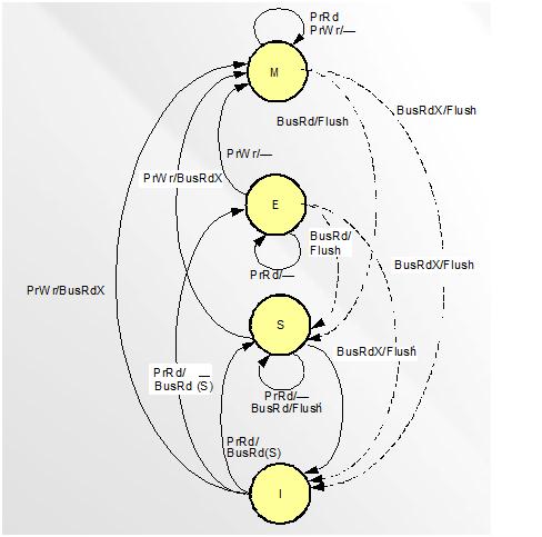
This figure shows the status change when bus traction generated. We are going to introduce those requests.
- PrRd: processors request to read a cache block.
- PrWr: processors request to write a cache block.
- BusRd: snooped request a read request to a cache block made by another processor.
- BusRdX: snooped request a read exclusive (write) request to a cache block made by another processor which doesn't already have the block. Shortly, write cache-to-memory
- BusUpgr: snooped request indicates that there is a write request to a cache block that another processor already has in its cache.
- Flush: snooped request indicates than an entire cache block is written back to main memory by another processors.
- FlushOpt: snooped request indicates that an entire block cache block is posted on the bus in order to supply it to another processor. Shortly, cache-to-cache.
Intel
Pentium processors include separate code and data caches integrated on-chip to meet performance goals. Each cache is 8 Kbytes in size, with a 32-byte line size and is 2-way set associative. Each cache has a dedicated Translation Lookaside Buffer (TLB) to translate linear addresses to physical addresses. The data cache is configurable to be write back or write through on a line-by-line basis and follows the MESI protocol.
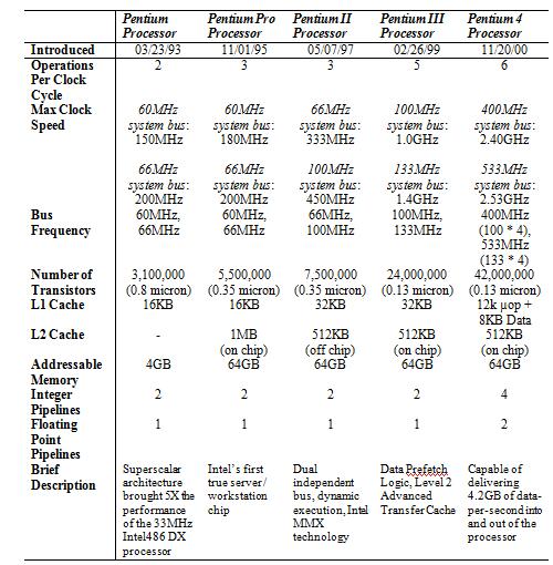
Each processor in the Pentium series incorporates and builds off of the previous processor’s architectural achievements. The following table summarizes the key enhancements found within each major Pentium processor starting with the original, released by Intel in 1993 to the most recent member of the Pentium family, the Pentium 4 processor.
Pentuum processor overview
The Pentium processor is the successor to the Intel486 processor. Originally released with a 66MHz clock speed, it is a 16-bit based superscalar processor capable of executing two instructions in parallel during a single clock. It uses a CISC (Complex Instruction Set Computer) type instruction set, and uses the little-endian type format to store bytes in memory. A 64-bit external bus, separate data and instruction caches, write buffers, and a pipelined floating-point unit combine to sustain a high executing rate. Caching along with pipeline and instruction flow are discussed below in detail.
Cache organization
L1 cache on the Pentium processor is 2-way set-associative in structure. In a set-associative structure the cache is divided into equal sections called cache ways. The cache page size is equal to the size of the cache way and each cache way is treated like a small direct mapped cache. In a 2-way scheme, two lines of memory may be stored at any time.
The Pentium processor’s cache line size is 32 bytes and is filled by a burst of four reads on the processor’s 64-bit data bus. Each cache way contains 128 cache lines and the cache page size is 4K, or 128 lines.
Cache operation modes
The data cache is configurable as a write-back or write-through on a line-by-line basis. The configuration of these two operation modes is initiated by either hardware or software with either the NW (Not Write-Through) bit set to 0 for the write-through mode or the NW bit set to 1 for the write-back mode. When the cache is configured as write-back, the cache acts like a buffer by receiving data from the processor and writing data back to main memory whenever the system bus is available. The advantage to the write-back process is that the processor is freed up to continue with other tasks while main memory is updated at a later time. However the disadvantage to this approach is that by having cache handle writes back to memory, the cost and complexity of cache subsequently increase. The second alternative is to configure the Pentium cache as write-through. In a write-through cache scheme the processor handles writes to main memory instead of the cache. The cache may update its contents as the data comes through from the processor however the write operation does not end until the processor has written the data back to main memory. The advantage to this approach is that the cache does not have to be as complex, which thus makes it less expensive to implement. The disadvantage of course is that the processor must wait until the main memory accepts the data before moving on to its next task.
Along with the NW (Not Write-Through) bit mentioned above, the other bit that allows for the control of the cache is the CD (Cache Disable) bit. As the name suggests, this bit allows for the hardware or the software to disable the cache. When the CD bit is set to 1 the cache is disabled and enabled when it is set to 0.
Cache consistency (MESI protocol)
The data cache supports the Cache Consistency Protocol, which is a set of rules by which states are assigned to cached entries or lines. The protocol consists of four states that define whether a line is valid (HIT or MISS), if it is available in other caches, and if it has been modified. The four states, which make up what is referred to as the MESI protocol, are the M (Modified), E (Exclusive), S (Shared) and the I (Invalid) states. The following is a description of each state:
An M-state line is modified meaning that it is different from main memory. An M-state line can also be accessed (read/written to) without sending a cycle out on the bus.
An E-state line is not modified. An E-state line can also be accessed (read/written to) without generating a bus cycle, with a write causing the line to become modified.
An S-state indicates that the line is potentially shared with other caches meaning that the same line may exist in more than one cache. Reading from this line does not generate bus activity however a write will generate a write-through cycle on the bus and may also invalidate this line in other caches. A write to an S-state line updates the cache.
An I-state indicates that the line is not available in cache. Reading from this line may cause a MISS and cause the processor to execute a LINE FILL where the whole line is fetched from main memory and placed back into cache. Writing to an INVALID line causes the processor to execute a write-through cycle on the bus.
The other piece of L1 cache, the code side, supports a subset of the MESI protocol, the S (Shared) and I (Invalid) states in order to prevent code from accidentally being corrupted since it is inherently write protected.
Here we will introduce how Intel implements MESI.
- Modified state
- a read will leave the line in the M state, and transfer the data to the CPU. - a write to a modified line will leave the line in the M state. The write is held in the cache. - snooping results in one of two transitions. Either the cache line is written back to RAM and marked shared, or it is written back to RAM and marked invalid, so that it can become exclusively held by another cache.
- Exclusive state
- a read will leave the line in the E state, and transfer the data to the CPU - a write will push the line into the modified state. The write is held in the cache. - snooping again results in one of two transitions, either to the shared or invalid state, for the same reasons as in state M.
- Shared state
- a read will leave the line in the S state, and transfer the data to the CPU - a write results in one of two transitions. Either the line becomes exclusively held by this cache resulting in a transition to state E (and I elsewhere), or this is a write-through cache and the update is sent to memory, and the line stays in state S. - snooping also results in one of two transitions, either back to shared or to invalid, for the same reasons as in state M.
- Invalid state
- a read results in one of three transitions. First, the data may be read into the cache to become exclusively held. Or the data may be read into the cache, and become shared. The third possibility is for a miss on a block that is exclusively held elsewhere; the block cannot be read, and the line remains invalid. - a write results in a miss, but there is no allowance for write-allocate on a miss in this protocol. The line remains invalid. - snooping results in a transition back to the invalid state, because the cache does not hold the data being checked for.
MOESI protocol (AMD)
MOESI basics
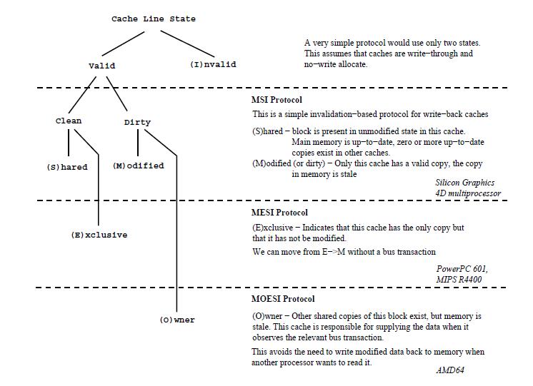
AMD Opteron is using MOESI (modified, owned, exclusive, shared, invalid) protocol for cache sharing. In addition to the four states in MESI, which is adopted by Intel for their Xeon processors, a fifth state "Owned" appears here representing data that is both modified and shared. Using MOESI, writing modified data back to main memory is avoided before being shared, which could save bandwidth and gain much faster access to users to the cache.
The states of the MOESI protocol are:
- Invalid—A cache line in the invalid state does not hold a valid copy of the data. Valid copies of the data can be either in main memory or another processor cache.
- Exclusive—A cache line in the exclusive state holds the most recent, correct copy of the data. The copy in main memory is also the most recent, correct copy of the data. No other processor holds a copy of the data.
- Shared—A cache line in the shared state holds the most recent, correct copy of the data. Other processors in the system may hold copies of the data in the shared state, as well. If no other processor holds it in the owned state, then the copy in main memory is also the most recent.
- Modified—A cache line in the modified state holds the most recent, correct copy of the data. The copy in main memory is stale (incorrect), and no other processor holds a copy.
- Owned—A cache line in the owned state holds the most recent, correct copy of the data. The owned state is similar to the shared state in that other processors can hold a copy of the most recent, correct data. Unlike the shared state, however, the copy in main memory can be stale (incorrect). Only one processor can hold the data in the owned state—all other processors must hold the data in the shared state.
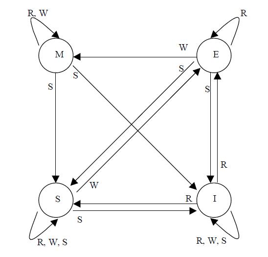
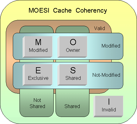
The figure below shows the five different states of MOESI protocol.
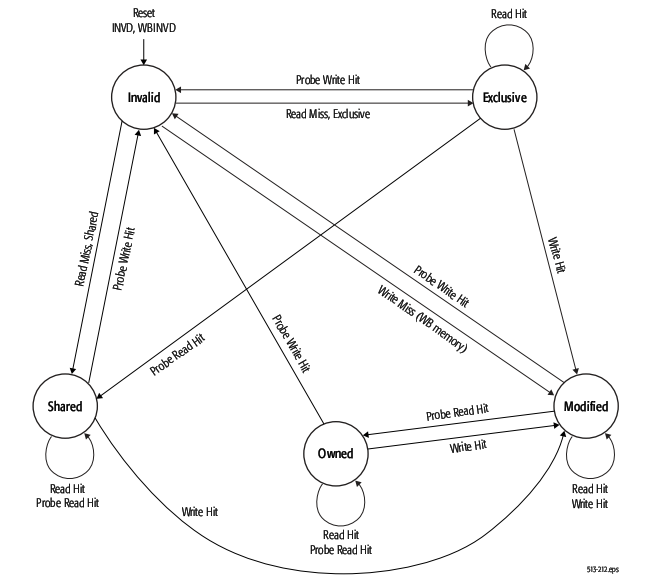
There are four valid states: M(odified) and E(xclusive) are not shared with other cache, while O(wned) and S(hared) with other caches. The state transitions of MOESI protocol is showed below:
AMD Special Coherency Considerations
In some cases, data can be modified in a manner that is impossible for the memory-coherency protocol to handle due to the effects of instruction prefetching. In such situations software must use serializing instructions and/or cache-invalidation instructions to guarantee subsequent data accesses are coherent. An example of this type of a situation is a page-table update followed by accesses to the physical pages referenced by the updated page tables. The following sequence of events shows what can happen when software changes the translation of virtual-page A from physical-page M to physical-page N:
- Software invalidates the TLB entry. The tables that translate virtual-page A to physical-page M are now held only in main memory. They are not cached by the TLB.
- Software changes the page-table entry for virtual-page A in main memory to point to physicalpage N rather than physical-page M.
- Software accesses data in virtual-page A. During Step 3, software expects the processor to access the data from physical-page N. However, it is possible for the processor to prefetch the data from physical-page M before the page table for virtualpage A is updated in Step 2. This is because the physical-memory references for the page tables are different than the physical-memory references for the data. Because the physical-memory references are different, the processor does not recognize them as requiring coherency checking and believes it is safe to prefetch the data from virtual-page A, which is translated into a read from physical page M. Similar behavior can occur when instructions are prefetched from beyond the page table update instruction.
To prevent this problem, software must use an INVLPG or MOV CR3 instruction immediately after the page-table update to ensure that subsequent instruction fetches and data accesses use the correct virtual-page-to-physical-page translation. It is not necessary to perform a TLB invalidation operation preceding the table update.
Dragon protocol
Intel
AMD
References
- Cache Coherence
- Cache consistency & MESI Intel
- A closer look at AMD's dual-core architecture
- CSE 400 – Related Work: Instructions & Example
- Trace-Driven Simulation of the MSI, MESI and Dragon Cache Coherence Protocols
- Understanding the Detailed Architecture of AMD's 64 bit Core
- MSI,MESI,MOESI sheet
- AMD64 Architecture Programmer’s Manual
- Intel PENTIUM
