CSC/ECE 506 Spring 2011/ch8 mc: Difference between revisions
| Line 251: | Line 251: | ||
[http://www.intel.com/technology/itj/2006/volume10issue02/art02_CMP_Implementation/p03_implementation.htm CMP Implementation in Intel Core Duo Processors] | [http://www.intel.com/technology/itj/2006/volume10issue02/art02_CMP_Implementation/p03_implementation.htm CMP Implementation in Intel Core Duo Processors] | ||
The '''Intel bus architecture''' has been '''evolving''' in order to accommodate the demands of scalability while using the '''same [http://en.wikipedia.org/wiki/MESI_protocol MESI] protocol'''; From using a '''single shared bus''' to '''dual independent buses (DIB)''' doubling the available bandwidth and to the logical conclusion of DIB with the introduction of '''dedicated high-speed interconnects (DHSI)'''. The DHSI-based platforms use four FSBs, one for each processor in the platform. In both DIB and DHSI, the snoop filter was used in the chipset to cache snoop information, thereby significantly reducing the broadcasting needed for the snoop traffic on the buses. With the production of processors based on next generation 45-nm Hi-k Intel Core microarchitecture, the [http://en.wikipedia.org/wiki/Xeon Intel Xeon] processor fabric will transition from a DHSI, with the memory controller in the chipset, to a distributed shared memory architecture using '''Intel QuickPath Interconnects using MESIF protocol'''. | The '''Intel bus architecture''' has been '''evolving''' in order to accommodate the demands of scalability while using the '''same [http://en.wikipedia.org/wiki/MESI_protocol MESI] protocol'''; From using a '''single shared bus''' to '''dual independent buses (DIB)''' doubling the available bandwidth and to the logical conclusion of DIB with the introduction of '''dedicated high-speed interconnects (DHSI)'''. The DHSI-based platforms use four FSBs, one for each processor in the platform. In both DIB and DHSI, the snoop filter was used in the chipset to cache snoop information, thereby significantly reducing the broadcasting needed for the snoop traffic on the buses. With the production of processors based on next generation 45-nm Hi-k Intel Core microarchitecture, the [http://en.wikipedia.org/wiki/Xeon Intel Xeon] processor fabric will transition from a DHSI, with the memory controller in the chipset, to a distributed shared memory architecture using '''Intel [http://en.wikipedia.org/wiki/Intel_QuickPath_Interconnect QuickPath Interconnects] using MESIF protocol'''. | ||
==AMD - Advanced Micro Devices Processors== | ==AMD - Advanced Micro Devices Processors== | ||
Revision as of 23:38, 17 April 2011
Introduction to bus-based cache coherence in real machines
Most parallel software in the commercial market relies on the shared-memory programming model in which all processors access the same physical address space. The most common multiprocessors today use SMP architecture which use a common bus as the interconnect. In the case of multicore processors ("chip multiprocessors," or CMP) the SMP architecture applies to the cores treating them as separate processors. The key problem of shared-memory multiprocessors is providing a consistent view of memory with various cache hierarchies. This is called cache coherence problem. It is critical to achieve correctness and performance-sensitive design point for supporting the shared-memory model. The cache coherence mechanisms not only govern communication in a shared-memory multiprocessor, but also typically determine how the memory system transfers data between processors, caches, and memory.
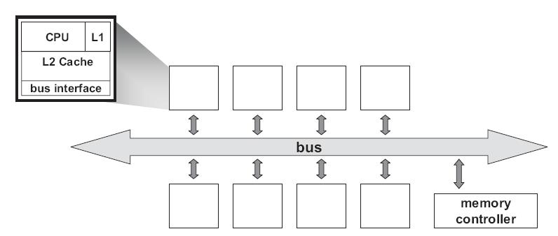
Cache Coherence in real machines
Summary of Cache Coherence Protocols
At any point in logical time, the permissions for a cache block can allow either a single writer or multiple readers. The coherence protocol ensures the invariants of the states are maintained. The different coherent states used by most of the cache coherent protocols are shown in Table 1:
| States | Access Type | Invariant |
| Modified | read, write | all other caches in I state |
| Exclusive | read | all other caches in I state |
| Owned | read | all other caches in I or S state |
| Shared | read | no other cache in M or E state |
| Invalid | - | - |
The first widely adopted approach to cache coherence is snooping on a bus. We will now discuss them in details in the following sections.
MSI
MSI protocol is a three-state write-back invalidation protocol which is one of the earliest snooping-based cache coherence-protocols. It marks the cache line with one of the Modified (M) ,Shared (S), and Invalid (I) state. Invalid means the cache line is either not present or is in invalid state. If the cache line is clean and is shared by more than one processor , it is marked as Shared. If a cache line is dirty and the processor has exclusive ownership of it, it is in Modified state. BusRdx causes other processors to invalidate (demote) its cache block to the I state. If it is present in the M state in another cache, it will flush.
The following state transition diagram for MSI protocol explains the working of the protocol:
MESI
MSI protocol has a major drawback in that each read-write sequence incurs two bus transactions irrespective of whether the cache line is stored in only one cache or not. This is a huge setback for highly parallel programs that have little data sharing. MESI protocol solves this problem by introducing the E (Exclusive) state to distinguish between a cache line stored in multiple caches and a line stored in a single cache. Let us briefly look at how the MESI protocol works. (For a more detailed version readers are referred to Solihin textbook pg. 215)
MESI coherence protocol marks each cache line in one of the Modified, Exclusive, Shared or Invalid state.
- Invalid : The cache line is either not present or is invalid
- Exclusive : The cache line is clean and is owned by this core/processor only
- Modified : This implies that the cache line is dirty and the core/processor has exclusive ownership of the cache line, exclusive of the memory also.
- Shared : The cache line is clean and is shared by more than one core/processor
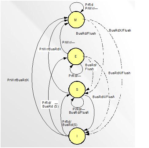
In a nutshell, the MESI protocol works as the following: A line that is just fetched receives E or S state depending on whether it exists in other processors in the system or not. Similarly, a cache line gets the M state when a processor writes to it. If the line is not in E or M state prior to being written to, the cache sends a Bus Upgrade (BusUpgr) signal or as the Intel manuals call it, a “Read-For-Ownership (RFO) request” that ensures that the line exists in the cache and is in the I state in all other processors on the bus (if any). The table shown below will summarize MESI protocol.
| Cache Line State: | Modified | Exclusive | Shared | Invalid |
| This cache line is valid? | Yes | Yes | Yes | No |
| The memory copy is… | out of date | valid | valid | - |
| Copies exist in caches of other processors? | No | No | Maybe | Maybe |
| A write to this line | does not go to bus | does not go to bus | goes to bus and updates cache | goes directly to bus |
Table 2: MESI Protocol Summary
The transition diagram from the lecture slides is given below for reference.
MESIF
The MESIF protocol, used in the latest Intel multi-core processors Core i7, was introduced to accommodate the point-to-point links used in the QuickPath Interconnect. Using the MESI protocol in this architecture would send many redundant messages between different processors, often with unnecessarily high latency. For example, when a processor requests a cache line that is stored in multiple locations, every location might respond with the data. As the requesting processor only needs a single copy of the data, the system would be wasting the bandwidth. As a solution to this problem, an additional state, Forward state, was added by slightly changing the role of the Shared state. Whenever there is a read request, only the cache line in the F state will respond to the request, while all the S state caches remain dormant. Hence, by designating a single cache line to respond to requests, coherency traffic is substantially reduced when multiple copies of the data exist. Also, on a read request, the F state transitions to the S state. That is, when a cache line in the F state is copied, the F state migrates to the newer copy, while the older one drops back to the S state. Moving the new copy to the F state exploits both temporal and spatial locality. Because the newest copy of the cache line is always in the F state, it is very unlikely that the line in the F state will be evicted from the caches. This takes advantage of the temporal locality of the request. The second advantage is that if a particular cache line is in high demand due to spatial locality, the bandwidth used to transmit that data will be spread across several cores. All M to S state transitions and E to S state transitions will now be from M to F and E to F. The F state is different from the Owned state of the MOESI protocol as it is not a unique copy because a valid copy is stored in memory. Thus, unlike the Owned state of the MOESI protocol, in which the data in the O state is the only valid copy of the data, the data in the F state can be evicted or converted to the S state, if desired.
More information on the QuickPath Interconnect and MESIF protocol can be found at Introduction to QuickPath Interconnect.
MOESI
AMD Opteron was AMD’s first-generation dual core processor which had two distinct K8 cores together on a single die. Cache coherence produces bigger problems on such multicore processors. It was necessary to use an appropriate coherence protocol to address this problem. The Intel Xeon, which was the competitive counterpart from Intel to AMD dual core Opteron, used the MESI protocol to handle cache coherence. MESI came with the drawback of using much time and bandwidth in certain situations.
MOESI was AMD’s answer to this problem. MOESI added a fifth state to MESI protocol called the owned state. MOESI protocol addresses the bandwidth problem faced by MESI protocol when processor having invalid data in its cache wants to modify the data. The processor seeking the data will have to wait for the processor which modified this data to write back to the main memory, which takes time and bandwidth. This drawback is removed in MOESI by allowing dirty sharing. When the data is held by a processor in the new state owned, it can provide other processors the modified data without writing it to the main memory. This is called dirty sharing. The processor with the data in the owned state stays responsible to update the main memory later when the cache line is evicted.
MOESI has become one of the most popular snoop-based protocols supported in AMD64 architecture. AMD dual-core Opteron can maintain cache coherence in systems up to 8 processors using this protocol.
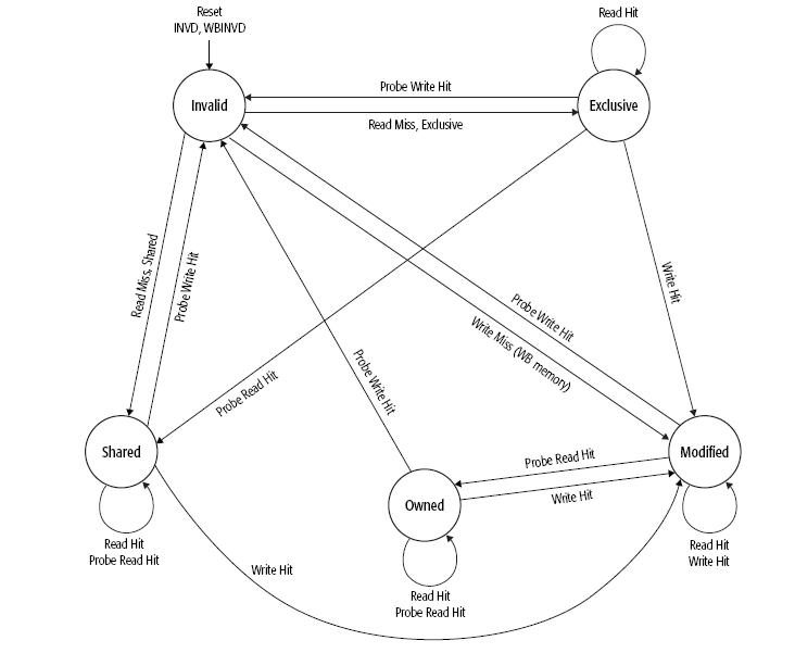
The five different states of MOESI protocol are:
- Modified (M): The most recent copy of the data is present in the cache line. But it is not present in any other processor cache.
- Owned (O): The cache line has the most recent correct copy of the data. This can be shared by other processors. The processor in this state for this cache line is responsible to update the correct value in the main memory before it gets evicted.
- Exclusive (E): A cache line holds the most recent, correct copy of the data, which is exclusively present on this processor and a copy is present in the main memory.
- Shared (S): A cache line in the shared state holds the most recent, correct copy of the data, which may be shared by other processors.
- Invalid (I): A cache line does not hold a valid copy of the data.
A detailed explanation of this protocol implementation on AMD processor can be found in the manual Architecture of AMD 64-bit core
The following table summarizes the MOESI protocol:
| Cache Line State: | Modified | Owner | Exclusive | Shared | Invalid |
| This cache line is valid? | Yes | Yes | Yes | Yes | No |
| The memory copy is… | out of date | out of date | valid | valid | - |
| Copies exist in caches of other processors? | No | No | Maybe | Maybe | - |
| A write to this line | does not go to bus | does not go to bus | goes to bus and updates cache | goes directly to bus | - |
Table 3: MOESI Protocol Summary
State transition for MOESIis as shown below :
We will now discuss which cache coherence protocol processor vendors like Intel, AMD and others adopt in various products.
Cache Coherence Protocols and Their Performance
Of all protocols, MSI appears to have the worst performance due to the fact that each read-write sequence incurs two bus transactions even if the data is stored in only one cache. This causes a huge performance penalty for highly optimized parallel programs that have little data sharing. MESI protocol solves this problem by introducing the E (Exclusive) state to distinguish between a cache line stored in multiple caches and a line stored in only one cache. This protocol, however, can still be improved further.
One remaining issue with MESI protocol is that in multi-processor configuration, when a processor requests a cache line that is stored in multiple cache, every cache might respond with the data. This behavior would waste bus bandwidth and incur high latency. As a solution to this problem, MESIF protocol was introduced. An additional state, Forward state, was added by slightly changing the role of the Shared state. The result of this improvement is that instead of all caches responding, only the cache line in the F state will respond to the request, while all the S state caches remain dormant. As a result, performance and power efficiency is increased.[23]
Another problem with MESI protocol is when a processor having invalid data in its cache wants to modify the data, it will have to wait for the other processor to write back to the memory, which is a very slow process. MOESI protocol solves this problem by allowing dirty sharing. This also saves bus bandwidth and increases performance.[24]
SGI - Silicon Graphics, Inc
MSI & SGI IRIS 4D Processors
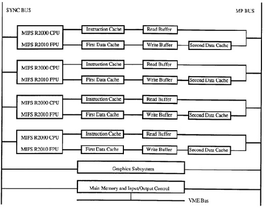
MSI protocol was first used in SGI IRIS 4D series. SGI produced a broad range of MIPS-based (Microprocessor without Interlocked Pipeline Stages) workstations and servers during the 1990s, running SGI's version of UNIX System V, now called IRIX. The 4D-MP graphics superworkstation brought 40 MIPS(million instructions per second) of computing performance to a graphics superworkstation. The unprecedented level of computing and graphics processing in an office-environment workstation was made possible by the fastest available Risc microprocessors in a single shared memory multiprocessor design driving a tightly coupled, highly parallel graphics system. Aggregate sustained data rates of over one gigabyte per second were achieved by a hierarchy of buses in a balanced system designed to avoid bottlenecks.
The multiprocessor bus used in 4D-MP graphics superworkstation is a pipelined, block transfer bus that supports the cache coherence protocol as well as providing 64 megabytes of sustained data bandwidth between the processors, the memory and I/O system, and the graphics subsystem. Because the sync bus provides for efficient synchronization between processors, the cache coherence protocol was designed to support efficient data sharing between processors. If a cache coherence protocol has to support synchronization as well as sharing, a compromise in the efficiency of the data sharing protocol may be necessary to improve the efficiency of the synchronization operations. Hence it uses the simple cache coherence protocol which is the MSI protocol.
With the simple rules of MSIprotocol enforced by hardware, efficient synchronization and efficient data sharing are achieved in a simple shared memory model of parallel processing in the 4D-MP graphics superworkstation.
SYNAPSE Multiprocessor
Synapse protocol and Synapse multiprocessor
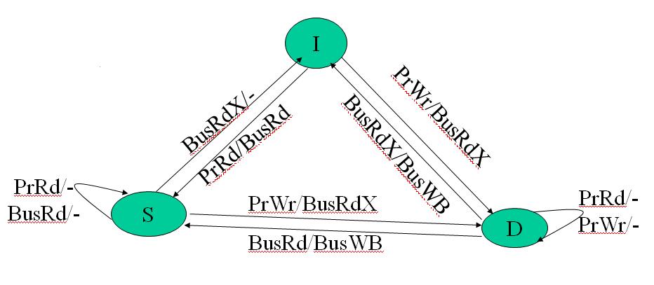
From the state transition diagram of MSI, we observe that for MSI there is transition to the S state from the M state when a BusRd is observed for that block. The contents of the block is flushed to the bus before going to S state. It would look more appropriate to move to the I state thus giving up the block entirely in certain cases. This choice of moving to S or I reflects the designer's assertion that the original processor is more likely to continue reading the block than the new processor to write to the block. In synapse protocol, used in the early Synapse multiprocessor, made this alternate choice of going directly from the M state to the I state on a BusRd, assuming the migratory pattern would be more frequent. More details about this protocol can be found in these papers published in late 1980's Coherence protocols: evaluation using a multiprocessor simulation model and Synapse tightly coupled multiprocessors: a new approach to solve old problems
In the Synapse protocol, the M state is called the D (Dirty) state. The following is the state transition diagram for Synapse protocol which clearly shows its working.
Intel
MESI & Intel Processors
The Pentium Pro microprocessor, introduced in 1992 was the first Intel architecture microprocessor to support symmetric multiprocessing (SMP) in various multiprocessor configurations. SMP and MESI protocol was the architecture used consistently until the introduction of the 45-nm Hi-k Core micro-architecture in Intel's (Nehalem-EP) quad-core x86-64. The 45-nm Hi-k Intel Core microarchitecture utilizes a new system of framework called the QuickPath Interconnect which uses point-to-point interconnection technology based on distributed shared memory architecture. It uses a modified version of MESI protocol called MESIF, by introducing an additional state, F, the forward state.
The Intel architecture uses the MESI protocol as the basis to ensure cache coherence, which is true whether you're on one of the older processors that use a common bus to communicate or using the new Intel QuickPath point-to-point interconnection technology.
CMP Implementation in Intel Architecture
Let us now see how Intel architecture using the MESI protocol progressed from a uniprocessor architecture to a Chip MultiProcessor (CMP) using the bus as the interconnect.
Uniprocessor Architecture
The diagram below shows the structure of the memory cluster in Intel Pentium M processor.
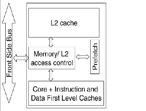
In this structure we have,
- A unified on-chip L1 cache with the processor/core,
- A Memory/L2 access control unit, through which all the accesses to the L2 cache, main memory and IO space are made,
- The second level L2 cache along with the prefetch unit and
- Front side bus (FSB), a single shared bi-directional bus through which all the traffic is sent across.These wide buses bring in multiple data bytes at a time.
As Intel explains it, using this structure, the processor requests were first sought in the L2 cache and only on a miss, were they forwarded to the main memory via the front side bus (FSB). The Memory/L2 access control unit served as a central point for maintaining coherence within the core and with the external world. It contains a snoop control unit that receives snoop requests from the bus and performs the required operations on each cache (and internal buffers) in parallel. It also handles RFO requests (BusUpgr) and ensures the operation continues only after it guarantees that no other version on the cache line exists in any other cache in the system.
CMP Architecture
For CMP implementation, Intel chose the bus-based architecture using snoopy protocols vs the directory protocol because though directory protocol reduces the active power due to reduced snoop activity, it increased the design complexity and the static power due to larger tag arrays. Since Intel has a large market for the processors in the mobility family, directory-based solution was less favorable since battery life mainly depends on static power consumption and less on dynamic power. Let us examine how CMP was implemented in Intel Core Duo, which was one of the first dual-core processor for the budget/entry-level market. The general CMP implementation structure of the Intel Core Duo is shown below
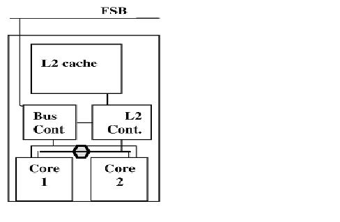
This structure has the following changes when compared to the uniprocessor memory cluster structure.
- L1 cache and the processor/core structure is duplicated to give 2 cores.
- The Memory/L2 access control unit is split into 2 logical units: L2 controller and bus controller. The L2 controller handles all requests to the L2 cache from the core and the snoop requests from the FSB. The bus controller handles data and I/O requests to and from the FSB.
- The prefetching unit is extended to handle the hardware prefetches for each core separately.
- A new logical unit (represented by the hexagon) was added to maintain fairness between the requests coming from the different cores and hence balance the requests to L2 and memory.
This new partitioned structure for the memory/L2 access control unit enhanced the performance while reducing power consumption. For more information on uniprocessor and multiprocessor implementation under the Intel architecture, refer to CMP Implementation in Intel Core Duo Processors
The Intel bus architecture has been evolving in order to accommodate the demands of scalability while using the same MESI protocol; From using a single shared bus to dual independent buses (DIB) doubling the available bandwidth and to the logical conclusion of DIB with the introduction of dedicated high-speed interconnects (DHSI). The DHSI-based platforms use four FSBs, one for each processor in the platform. In both DIB and DHSI, the snoop filter was used in the chipset to cache snoop information, thereby significantly reducing the broadcasting needed for the snoop traffic on the buses. With the production of processors based on next generation 45-nm Hi-k Intel Core microarchitecture, the Intel Xeon processor fabric will transition from a DHSI, with the memory controller in the chipset, to a distributed shared memory architecture using Intel QuickPath Interconnects using MESIF protocol.
AMD - Advanced Micro Devices Processors
MOESI & AMD Processors
AMD Opteron memory Architecture
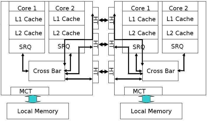
The AMD processor’s high-performance cache architecture includes an integrated, 64-bit, dual-ported 128-Kbyte split-L1 cache with separate snoop port, multi-level translation lookaside buffers (TLBs), a scalable L2 cache controller with a 72-bit (64-bit data + 8-bit ECC) interface to as much as 8-Mbyte of industry-standard SDR or DDR SRAMs, and an integrated tag for the most cost-effective 512-Kbyte L2 configurations. The AMD Athlon processor’s integrated L1 cache comprises two separate 64-Kbyte, two-way set-associative data and instruction caches.
More information about this can be found in AMD 64 bit Architecture Programmers's Manual
Special Coherence Considerations in AMD64 architectures
Instruction prefetching is a technique used to speedup the execution of the program. But in multiprocessors, prefetching comes at the cost of performance. Due to prefetching, the data can be modified in such a way that the memory coherence protocol will not be able to handle the effects. In such situations software must use serializing instructions or cache-invalidation instructions to guarantee subsequent data accesses are coherent.
An example of this type of a situation is a page-table update followed by accesses to the physical pages referenced by the updated page tables. The physical-memory references for the page tables are different than the physical-memory references for the data. Because of prefetching, there maybe problem with correctness. The following sequence of events shows such a situation when software changes the translation of virtual-page A from physical-page M to physical-page N:
- The tables that translate virtual-page A to physical-page M are now held only in main memory. The copies in the cache ae invalidated.
- Page-table entry is changed by the software for virtual-page A in main memory to point to physical page N rather than physical-page M.
- Data in virtual-page A is accessed.
Software expects the processor to access the data from physical-page N after the update. However, it is possible for the processor to prefetch the data from physical-page M before the page table for virtual page A is updated. Because the physical-memory references are different, the processor does not recognize them as requiring coherence checking and believes it is safe to prefetch the data from virtual-page A, which is translated into a read from physical page M. Similar behavior can occur when instructions are prefetched from beyond the page table update instruction.
In order to prevent errors from occuring, there are special instructions provided by software like INVLPG or MOV CR3 instruction which is executed immediately after the page-table update to ensure that subsequent instruction fetches and data accesses use the correct virtual-page-to-physical-page translation. It is not necessary to perform a TLB invalidation operation preceding the table update.
More information can be found about this in AMD64 Architecture Programmer's manual
Optimization techniques on MOESI when implemented on AMD Phenom processors
In real machines, using some optimization techniques on the standard cache coherence protocol used, improves the performance of the machine. For example, AMD Phenom family of microprocessors (Family 0×10) which is AMD’s first generation to incorporate 4 distinct cores on a single die. It is the first to have a cache that all the cores share, using the MOESI protocol with some optimization techniques incorporated.
It focuses on a small subset of compute problems which behave like Producer and Consumer programs. In such a computing problem, a thread of a program running on a single core produces data, which is consumed by a thread that is running on a separate core. With such programs, it is desirable to get the two distinct cores to communicate through the shared cache, to avoid round trips to/from main memory. The MOESI protocol that the AMD Phenom cache uses for cache coherence can also limit bandwidth. Hence by keeping the cache line in the M state for such computing problems, we can achieve better performance.
When the producer thread , writes a new entry, it allocates cache-lines in the M state. Eventually, these M-marked cache lines will start to fill the L3 cache. When the consumer reads the cache line, the MOESI protocol changes the state of the cache line to the O state in the L3 cache and pulls down a shared (S) copy for its own use. Now, the producer thread circles the ring buffer to arrive back to the same cache line it had previously written. However, when the producer attempts to write new data to the owned (marked ‘O’) cache line, it finds that it cannot, since a cache line in the O state by the previous consumer read does not have sufficient permission for a write request (in the MOESI). To maintain coherence, the memory controller must initiate probes in the other caches (to handle any other S copies that may exist). This will slow down the process.
Thus, it is preferable to keep the cache line in the M state in the L3 cache. In such a situation, when the producer comes back around the ring buffer, it finds the previously written cache line still in theM state, to which it is safe to write without coherence concerns. Thus better performance can be achieved by such optimization techniques to standard protocols when implemented in real machines.
You can find more information on how this is implemented and various other ways of optimizations in this manual Software Optimization guide for AMD 10h Processors.
Xerox Corporation
Dragon Protocol & Xerox Dragon Processors
The Dragon Protocol is an update based coherence protocol which does not invalidate other cached copies like what we have seen in the coherence protocols so far. Write propagation is achieved by updating the cached copies instead of invalidating them. But the Dragon Protocol does not update memory on a cache to cache transfer and delays the memory and cache consistency until the data is evicted and written back, which saves time and lowers the memory access requirements. Moreover only the written byte or the word is communicated to the other caches instead of the whole block which further reduces the bandwidth usage. It has the ability to detect dynamically, the sharing status of a block and use a write through policy for shared blocks and write back for currently non-shared blocks. The Dragon Protocol employs the following four states for the cache blocks: Shared Clean, Shared Modified, Exclusive, and Modified.
- Modified (M) and Exclusive (E) - these states have the same meaning as explained in the protocols above.
- Shared Modified (Sm) - Only one cache line in the system can be in the Shared Modified state. Potentially two or more caches have this block and memory may or may not be up to date and this processor's cache had modified the block.
- Shared Clean (Sc) - Potentially two or more caches have this block and memory may or may not be up to date(if no other cache has it in Sm state, memory will be up to date else it is not).
When a Shared Modified line is evicted from the cache on a cache miss only then is the block written back to the main memory in order to keep memory consistent. For more information on Dragon protocol, refer to Solihin textbook, page number 229. The state transition diagram has been given below for reference.
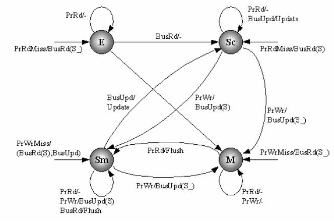
The Dragon Protocol , was developed by Xerox Palo Alto Research Center (Xerox PARC), a subsidiary of Xerox Corporation. This protocol was used in the Xerox PARC Dragon multiprocessor workstation, a VLSI research computer that could support multiple processors on a central high bandwidth memory bus. The Dragon design implemented snoopy caches that provided the appearance of a uniform memory space to multiple processors. Here, each cache listens to 2 buses: the processor bus and the memory bus. The caches are also responsible for address translation, so the processor bus carries virtual addresses and the memory bus carries physical addresses. The Dragon system was designed to support 4 to 8 Dragon processors. The memory bus used in the Xeron Dragon evolved to become the XDBus , a low-cost, synchronous, packet-switched VLSI bus designed for use in high-performance multiprocessors. This was used as the interconnect in many multiprocessor server systems like Cray Superserver 6400, Sun Microsystems' SPARCcenter 2000 and SPARCserver 1000 and Sun4d systems.
Cache Coherence Power Utilization
A number of studies have been performed to reduce the power consumption of cache coherence protocols. In order to perform a solid comparison between the cache coherency protocols, one would need to develop a multi-core processor for each of the cache coherency protocols. Additionally, the hardware and software configuration would also need to be similar between each system (except for the hardware required to implement each of the different protocols). Unfortunately, there are no such processors available. This section will discuss power consumption in general terms, comparing to each of the protocols. Also, this section will briefly discussion some power optimization techniques.
Bus transactions, in general, are costly for both performance and power consumption. Additionally, studies have been performed showing that unnecessary snooping can waste power. Power requirements are typically determined by the number of bus snoops and number of bus accesses by each processor. One study indicates that interchip bus communications can consume up to 20% of total chip power[20]. Using the examples from the class notes, we can analyze the relative power consumption between the protocols. The following table is a summary of various protocols showing the number of bus communications that occur for each processor action.
| Processor Action | MSI Bus Actions | MESI Bus Actions | Dragon Bus Actions | FireFly Bus Actions |
| R1 | BusRd | BusRd | BusRd | BusRd |
| W1 | BusRdX | |||
| R3 | BusRd/Flush | BusRd/Flush | BusRd/Flush | BusRd/Flush |
| W3 | BusRdX | BusRdX | BusUpd/Upd | BusUpd |
| R1 | BusRd/Flush | BusRd/Flush | ||
| R3 | ||||
| R2 | BusRd | BusRd | BusRd/Flush | BusRd/Flush |
Table 4: Summary of Bus Actions for Select Protocols
From the table above, we can see that MSI has a larger number of bus transactions than the Dragon protocol. Even though bus transactions are not power efficient, snooping can also be enhanced to improve power efficiency. The following section will discuss snoop filtering techniques.
Power Savings Using Snoop Filtering
A number of studies have been performed to reduce the number of unnecessary snoops during cache transactions. Two such filtering techniques are serial snooping and Jetty. The following sections will briefly discuss these two filtering techniques and power savings achieved using these techniques. Studies show that as much as 90% of snoop broadcasts will result in a miss[19] in the other caches at the same level and require that the information be provided by the next level of cache or memory. As much as a 36% savings in power by filtering snoops using one of the following snoop filtering methods[19].
Serial Snooping
Serial snooping takes advantage of the fact that if a miss occurs in one cache, it is possible to find the block in one other cache without having to check all the caches. If the cache block is available in multiple caches, there is a high probability that the cache miss can find the data in a nearby cache. Alternatively, savings can be realized by searching a subset of the caches vice all the caches. One thing to note is that this is only effective for read misses. Write, an invalidation transaction needs to be transmitted to the other caches, thus a bus transaction is unavoidable.
Jetty
Jetty is a mechanism attached to each cache that verifies that a bus snoop is necessary. Jetty is used to filter L2 tag lookups. When a processor needs to perform a bus snoop, the Jetty is checked first. The Jetty can determine if a cache tag lookup is required. Since the Jetty is much smaller than the associated cache, less power is required to determine if a snoop is required.
There are a couple of different Jetty schemes. There is the exclude-Jetty, include-Jetty, and hybrid-Jetty. The exclude-Jetty exploits the fact that if a cache block is snooped, it is highly likely the same cache block will be snooped in the near future. The exclude-Jetty keeps track of the tag lookups in a small table and can determine if a cache tag lookup is necessary.
The include-Jetty keeps a superset of the blocks that are cached. If a miss occurs in the include-Jetty, then it can be guaranteed that the block is not stored in its associated cache.
The hybrid-Jetty is simply a combinations of and include and exclude-Jetty. Both types of Jetty are present and when a lookup occurs, both Jettys are checked to determine if a cache lookup is necessary.
References
- Cache coherence
- Introduction to QuickPath Interconnect
- CMP Implementation in Intel Core Duo Processors
- Common System Interface in Intel Processors
- Cache consistency with MESI on Intel processor
- AMD dual core Architecture
- AMD64 Architecture Programmer's manual
- Software Optimization guide for AMD 10h Processors
- Architecture of AMD 64 bit core
- Silicon Graphics Computer Systems
- Parallel computer architecture: a hardware/software approach By David E. Culler, Jaswinder Pal Singh, Anoop Gupta
- Three state invalidation protocols
- Synapse tightly coupled multiprocessors: a new approach to solve old problems
- Coherence protocols: evaluation using a multiprocessor simulation model
- Dragon Protocol
- Xerox Dragon
- Coherence Protocols
- XDBus
- Evaluation of Snoop-Energy Reduction Techniques for Chip-Multiprocessors
- Power Efficient Cache Coherence
- The Common System Interface: Intel's Future Interconnect
- AMD64 Architecture Programmer's Manual Vol 2 'System Programming'
- 'The research of the inclusive cache used in multi-core processor' by Bin-feng Qian and Li-min Yan.
- 'Comparing cache architectures and coherency protocols on x86-64 multicore SMP systems' by Hackenberg, D., Molka, D. and Nagel, W.E.