CSC/ECE 506 Spring 2010/chapter 8: Difference between revisions
No edit summary |
No edit summary |
||
| Line 66: | Line 66: | ||
|- | |- | ||
| Cache Line State: | | '''Cache Line State:''' | ||
| Modified | | '''Modified''' | ||
| Owner | | '''Owner''' | ||
| Exclusive | | '''Exclusive''' | ||
| Shared | | '''Shared''' | ||
| Invalid | | '''Invalid''' | ||
|- | |- | ||
| This cache line is valid? | | '''This cache line is valid?''' | ||
| Yes | | Yes | ||
| Line 94: | Line 94: | ||
|- | |- | ||
| The memory copy is… | | '''The memory copy is…''' | ||
| out of date | | out of date | ||
| Line 108: | Line 108: | ||
|- | |- | ||
| Copies exist in caches of other processors? | | '''Copies exist in caches of other processors?''' | ||
| No | | No | ||
| Line 120: | Line 120: | ||
|- | |- | ||
| A write to this line | | '''A write to this line''' | ||
| does not go to bus | | does not go to bus | ||
Revision as of 22:36, 26 March 2010
Introduction to Bus-based cache coherency in real machines
Background
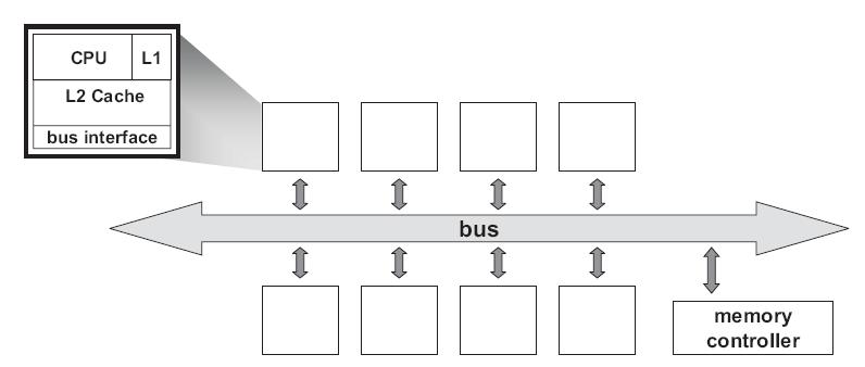
Most parallel software in the commercial market relies on the shared-memory programming model in which all processors access the same physical address space. And the most common multiprocessors today use SMP architecture which use a common bus as the interconnect. In the case of multicore processors (CMP) the SMP architecture applies to the cores treating them as separate processors. The key problem of shared-memory multiprocessors is providing a consistent view of memory with various cache hierarchies. This is called cache coherence problem. It is critical to achieve correctness and performance-sensitive design point for supporting the shared-memory model. The cache coherence mechanisms not only govern communication in a shared-memory multiprocessor, but also typically determine how the memory system transfers data between processors, caches, and memory.
Figure 1 : Bus-Based symmetric multiprocessors
At any point in logical time, the permissions for a cache block can allow either a single writer or multiple readers. The coherence protocol ensures the invariants of the states are maintained. The different coherent states used by most of the cache coherent protocols are as shown in Table 1:
| States | Access Type | Invariant |
| Modified | read, write | all other caches in I state |
| Exclusive | read | all other caches in I state |
| Owned | read | all other caches in I or S state |
| Shared | read | no other cache in M or E state |
| Invalid | - | - |
Table 1
The first widely adopted approach to cache coherence is snooping on a bus. We will now discuss how some real time machines by Intel and AMD maintains cache coherence using snooping based coherence protocols. For more information on snooping based protocols refer to Solihin text book Chapter 8.
Cache Coherency on real machines
AMD - Advanced Micro Devices Processors
MOESI on AMD64 Processors
AMD Opteron was the AMD’s first generation dual core which had 2 distinct K8 cores together on a single die. Cache coherence produces bigger problems on such multiprocessors. It was necessary to use an appropriate coherence protocol to address this problem. Intel Xeon which was the competitive counterpart from Intel to AMD dual core Opteron , used MESI protocol to handle cache coherence problem. MESI came with a drawback of using much time and bandwidth in certain situations.
MOESI was the AMD’s answer to this problem . MOESI added a fifth state to MESI protocol called “Owned” . MOESI addresses the bandwidth problem faced in MESI protocol when processor having invalid data in its cache wants to modify the data. The processor seeking the data access will have to wait for the processor which modified this data to write back to the main memory which takes time and bandwidth. This drawback is removed in MOESI by allowing dirty sharing. When the data is held by a processor in the new state “Owned”, it can provide other processors the modified data without or even before writing it to the main memory. This is called dirty sharing. The processor with the data in "Owned" stays responsible to update the main memory later when the cache line is evicted.
MOESI has become one of the most popular snoop based protocol supported in AMD64 architecture. The AMD dual core Opteron can maintain cache coherency in systems upto 8 processors using this protocol.
The five different states of MOESI protocol are:
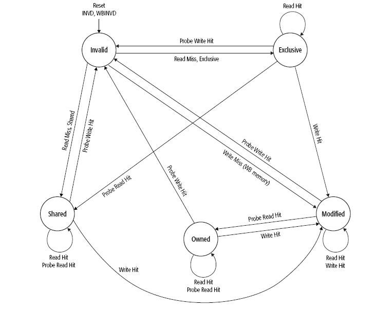
- Modified(M) : The most recent copy of the data is present in the cache line. But it is not present in any other processor cache.
- Owned (O) : The cache line has the most recent correct copy of the data . This can be shared by other processors. The processor in this state for this cache line is responsible to update the correct value in the main memory before it gets evicted.
- Exclusive (E) : A cache line holds the most recent, correct copy of the data, which is exclusively present on this processor and a copy is present in the main memory.
- Shared (S) : A cache line in the shared state holds the most recent, correct copy of the data, which may be shared by other processors.
- Invalid (I) : A cache line does not hold a valid copy of the data.
The following table summarizes the MOESI protocol:
| Cache Line State: | Modified | Owner | Exclusive | Shared | Invalid |
| This cache line is valid? | Yes | Yes | Yes | Yes | No |
| The memory copy is… | out of date | out of date | valid | valid | - |
| Copies exist in caches of other processors? | No | No | Yes(out of date values) | Maybe | Maybe |
| A write to this line | does not go to bus | does not go to bus | does not go to bus | goes to bus and updates cache | goes directly to bus |
State transition for MOESI is as shown below in Figure 2 :
Figure 2 : MOESI State transition Diagram
AMD Opteron memory Architecture
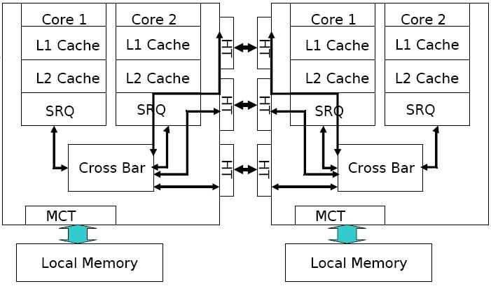
Figure 3 : Memory Architecture in dual core AMD Opteron
The AMD processor’s high-performance cache architecture includes an integrated, 64-bit, dual-ported 128-Kbyte split-L1 cache with separate snoop port, multi-level translation lookaside buffers (TLBs), a scalable L2 cache controller with a 72-bit (64-bit data + 8-bit ECC) interface to as much as 8-Mbyte of industry-standard SDR or DDR SRAMs, and an integrated tag for the most cost-effective 512-Kbyte L2 configurations. The AMD Athlon processor’s integrated L1 cache comprises two separate 64-Kbyte, two-way set-associative data and instruction caches.
Special Coherency Considerations in AMD64 architectures
In some cases, data can be modified in a manner that is impossible for the memory-coherency protocol to handle due to the effects of instruction prefetching. In such situations software must use serializing instructions and/or cache-invalidation instructions to guarantee subsequent data accesses are coherent. An example of this type of a situation is a page-table update followed by accesses to the physical pages referenced by the updated page tables. The following sequence of events shows what can happen when software changes the translation of virtual-page A from physical-page M to physical-page N:
- Software invalidates the TLB entry. The tables that translate virtual-page A to physical-page M are now held only in main memory. They are not cached by the TLB.
- Software changes the page-table entry for virtual-page A in main memory to point to physical page N rather than physical-page M.
- Software accesses data in virtual-page A.
During Step 3, software expects the processor to access the data from physical-page N. However, it is possible for the processor to prefetch the data from physical-page M before the page table for virtual page A is updated in Step 2. This is because the physical-memory references for the page tables are different than the physical-memory references for the data. Because the physical-memory references are different, the processor does not recognize them as requiring coherency checking and believes it is safe to prefetch the data from virtual-page A, which is translated into a read from physical page M. Similar behavior can occur when instructions are prefetched from beyond the page table update instruction.
To prevent this problem, software must use an INVLPG or MOV CR3 instruction immediately after the page-table update to ensure that subsequent instruction fetches and data accesses use the correct virtual-page-to-physical-page translation. It is not necessary to perform a TLB invalidation operation preceding the table update.
Optimizing Inter-Core Data Transfer on AMD Phenom(TM) processors by using some optimization technique on MOESI
The AMD Phenom family of microprocessors (Family 0×10) is AMD’s first generation to incorporate 4 distinct cores on a single die, and the first to have a cache that all the cores share. There is a small subset of compute problems that can be categorized as belonging in a Producer and Consumer paradigm; a thread of a program running on a single core produces data, which is meant to be consumed by a thread that is running on a separate core. With such programs, it is desirable to get the two distinct cores to communicate through the shared cache, to avoid round trips to/from main memory. The MOESI protocol that the AMD Phenom cache uses for cache coherency can also limit bandwidth; it is important to keep a cache line in the ‘M’ state for optimal producer/consumer performance. The producer thread allocates cache-lines in the modified (M) state, as an automatic consequence of writing a new entry. Eventually, these M-marked cache lines will start to fill the L3 cache, according to the rules defining the allowable distance between threads. When the consumer reads the cache line, the MOESI protocol changes the state of the cache line to owned (O) in the L3 cache and pulls down a shared (S) copy for its own use. Now, the producer thread circles the ring buffer to arrive back to the same cache line it had previously written. However, when the producer attempts to write new data to the owned (marked ‘O’) cache line, it finds that it cannot, since a cache line marked ‘O’ by the previous consumer read does not have sufficient permission for a write request (in the MOESI parlance). To maintain coherence, the memory controller must initiate probes in the other caches (to handle any other S copies that may exist)—and this is slow.
Thus, it is preferable to keep the cache line in the ‘M’ state in the L3 cache. Then, when the producer comes back around the ring buffer, it finds the previously written cache line still marked ‘M’, to which it is safe to write without coherency concerns.
Thus a producer/consumer program can achieve harmony by successfully bouncing an ‘M’ marked cache line back and forth between the consuming and producing threads through the fast L3 cache. The constraints to keep in mind to achieve this behavior are as follows:
- The consumer thread needs to ‘lag’ the producer thread by at least L1 + L2 cache size (modulo arithmetic).
- The producer thread needs to lag the consumer thread by at least L1 + L2 cache size (modulo arithmetic).
- The ring buffer should be at least 2 × (L1 + L2).
- The producer thread should not get so far ahead of the consumer to flood the L3, if larger ring buffers are used.
- Use PREFETCHW on the consumer side, even if the consumer will not modify the data.
- Add a small extra factor to the calculated sizes to give the threads additional space when communicating through the caches.


