CSC/ECE 506 Fall 2007/wiki1 4 JHSL: Difference between revisions
| Line 20: | Line 20: | ||
[[Image:250px-Types_of_Carbon_Nanotubes.png|thumb|Carbon nanotubes, from http://en.wikipedia.org/wiki/Carbon_nanotube]] | [[Image:250px-Types_of_Carbon_Nanotubes.png|thumb|Carbon nanotubes, from http://en.wikipedia.org/wiki/Carbon_nanotube]] | ||
=== The Future is here: Carbon nanotubes === | === The Future is here: Carbon nanotubes === | ||
While | While silicon is still the primary choice for today's technology, a new material has attracted attention of the semiconductor industry--carbon nanotubes. Carbon nanotubes are microscopic cylinders of only about 1nm in diameter, and possess very interesting electrical properties. Under some conditions they can be metallic, and under other conditions they act as semiconductors. In 2001, IBM was successful in constructing first carbon-based transistors [3]. | ||
<br clear="all"> | <br clear="all"> | ||
Revision as of 01:34, 6 September 2007
Architectual Trends
General trends
During the last ten years, general architectural trends did not change much: logic density is still increasing, number of CPUs per machine is rising, and memory size and bandwidth are growing. The only difference is that most of the yesterday's bleeding-edge technologies have made their way to the consumer market. They are now available for individual users, not just big companies and research centers. Ready availability of such technologies, in turn, has fed the hi-end portion of the market, and today the commodity parts are the preferred choices for the state-of-the art computer building.
While general direction is still the same, it is important to note some of the technological advances that could potentially set the direction for the next generation of computers. In this article, the bottom-up approach will be used to discuss architectural trends--major advancements in the underlying technology will be mentioned first, and discussion of the higher-level architecture will follow.
"Rock bottom" (Silicone/Carbon)
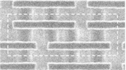
Trend of a transistor size
The very basic building block of electronic technology, the transistor, has shrunk dramatically during the past decade. Processors built on 45nm technology are widely available on the market. According to Intel's press release from the beginning of this year, "Just a decade ago, the state-of-the-art process technology was 250nm, meaning transistor dimensions were approximately 5.5 times the size and 30 times the area of the technology announced today by Intel" [1].
It is worth mentioning that while 45nm is current production specification, all major players have already announced plans to decrease trace width even further.
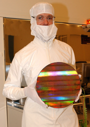
Wafer size and CPU footprint
While the transistor size continues to decrease, manufacturers have been consistently moving towards larger silicon wafer sizes. Today, most of the CPUs are produced on 300mm wafers. Combined with increased logic density, this allows manufacturers to produce more processors from a single wafer, therefore significantly decreasing overall production costs.
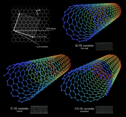
The Future is here: Carbon nanotubes
While silicon is still the primary choice for today's technology, a new material has attracted attention of the semiconductor industry--carbon nanotubes. Carbon nanotubes are microscopic cylinders of only about 1nm in diameter, and possess very interesting electrical properties. Under some conditions they can be metallic, and under other conditions they act as semiconductors. In 2001, IBM was successful in constructing first carbon-based transistors [3].
Longer, Wider, Deeper and Smarter:
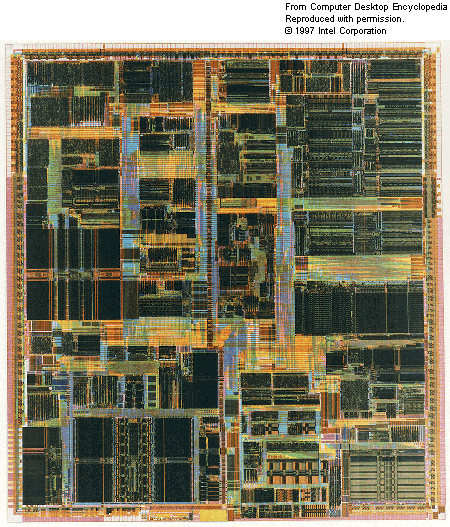
Ever decreasing transistor sizes has enabled design of ever more complex processors. In 1995, Intel has released its biggest CPU up to that date, Pentium PRO. Based on revolutionary P6 design, it introduced such features as speculative execution, super pipelining and register renaming to x86 world for the first time. Pentium PRO's better known reincarnation, Pentium II, have been introduced to mass market in 1997 represented one of the best and longer-running CPU architectures developed by Intel. As can be seen on the diagram below, it has five distinct execution units, controlled by the out-of-order execution logic. This allowed Pentium-II CPUs to execute up to 5 uOPS per each clock cycle. Combined with deep high-clock, 12-stage pipeline, the CPU provided superior performance.
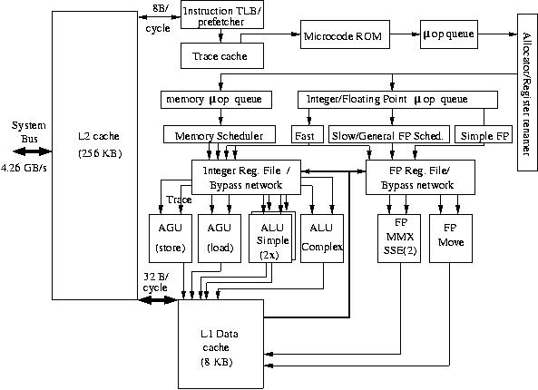
Longer pipelines (Intel Netburst)
Encouraged by success of long pipeline in P6 architecture, Intel decided to push it even further. In November 2000, new "Netburst" technology was introduced to the market as Pentium 4. This CPU have been completely redesigned, and featured extremely long, 31-stage pipeline that could run at clock speeds of up to 4GHz.
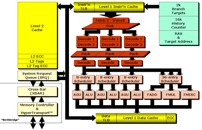
Wider internal buses, more logical units
While Intel was engaged into the chase after The Gigahertz, AMD took another approach to increasing CPU performance. With new design, AMD K8 had much shorter pipeline (11 steps for integers units and 17 steps for floating point), compared to 31 of Intel Pentium 4. This means that each stage has to do more work, therefore not capable of such high clock speeds as it's rival. However, what K8 lacked in clock cycles per second, it picked up in number of instructions executed per clock cycle. A simple look at K8's architectural diagram reveals that AMD, in some sense, succeeded to glue together three nearly complete cores in a single CPU:
There are three of everything: decoders, schedules, ALU/AGU, and FPU units (although not all of them are equal in functionality).
Deeper caches
As core clock speeds skyrocketed, so did the need for fast memory access. However, since front-side buses were not in position to deliver the bandwidth, and more importantly, short response times required by modern CPUs, the industry turned to caching. In relatively short period of time cache sizes grew from 128KB to 512KB and then even to several megabytes. For some CPUs FSB bandwidth problem became so critical that not only cache size have been increased, but also a whole extra L3 layer of caching have been added. Today it is not unusual to see a system with 8MB of L2 cache (Intel Core 2 Quad) or even 24MB of L3 cache (Intel Itanium 2 9050).
"Smarter" CPUs

Not only CPUs became smaller, faster and capable of performing multiple instructions per cycle, but they also became smarter about how they perform instructions. As a rule, practically all modern CPUs implement in hardware such elaborate mechanisms as branch prediction, speculative execution, register renaming and out-of-order execution. But as we all know, there are no rules without exceptions, and one of the most interesting exceptions is Intel Itanium. Instead of complex logic implementation, it has the ability to read "hints" generated by a compiler from the code stream, and make decisions based on that information. This approach allowed to replace "fixed" rules embedded in silicone with flexibility of a compiler that could perform far more complex analysis
Another interesting development is introduction of a built-in memory controller in Opteron processors by AMD. This feature allowed CPU to manage all memory access the way it sees fit, ensuring that other components cannot delay memory requests coming from the CPU.
"My dual quad-core with quad-SLI"
Since there is a limit on number of execution units in the CPU after which there is no significant performance gain, processor manufacturers were forced to shift their attention from instruction-level parallelism to thread-level. The following sections takes a closer look at some of the recent thread-level developments.
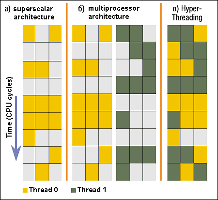
Intel Hyperthreading
The first commodity processor that could handle multiple threads at the same time was Intel Pentium 4 with HyperThreading (HT) technology. The basic idea behind the HT is to keep the same number of execution units in CPU, but double the register file and some control logic to allow two threads to share the resources of a single CPU.
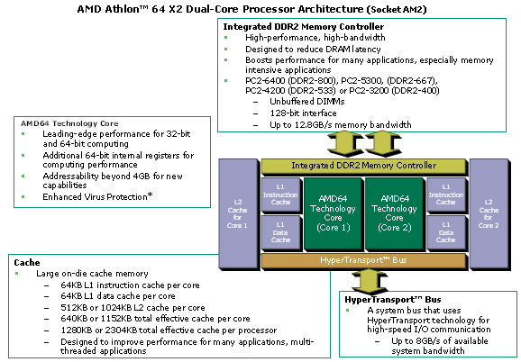
Intel Core 2 Duo, AMD X2
The next logical step after HyperThreading was full-scale multi-core design. While Intel rushed to put two separate cores connected via FSB in the same package, AMD held off it's own dual core CPU in order to develop it right. As a result, AMD came to the market later, but with better, "real" Dual-core CPU, not just two separate cores in the same packaging.
Shortly thereafter, Intel released it's revised dual-code processor, this time designed similarly to AMD. It is important to note that both manufacturers have strong plans to increase the number of cores per package, and Intel has already released it's first Quad-Code CPUs.
Cell
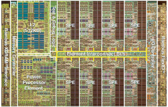
In 2001, Sony, Toshiba, and IBM (collectively known as "STI") began working on the Cell Broadband Engine Architecture ("cell") processor. It contains general-purpose RISC-based processor cores and a set of highly-specialized coprocessors which can handle multimedia and vector processing tasks with high efficiency. The engineers of the cell processor chose to favor power efficiency, high bandwidth, and computational speed over ease of development, which has led some to claim that the platform is difficult to use in development. The cell processor was widely distributed as part of the Sony PlayStation 3 gaming console, in a configuration with a single general-purpose processor with seven coprocessors.
Sun Niagara
If you think that having two dual-core CPUs with HyperThreading in the same box is insane or having seven co-processors is a bit excessive, think again. Buy introduction of it's Niagara technology, Sun Microsystems made the whole notion of number of CPUs in a box irrelevant. This monster has four UltraSparc cores in a single package and is capable of running 4 threads per core. If this is not enough, it is possible to have multiple CPUs in the same system. Sun positioned the chip as environmentally friendly, since it consumed only 70 watts of power, far less than comparable chips in the market. The Niagara processor was released in 2005 as the Sun "UltraSPARC T1".
Attempting to build on the success of the UltraSPARC T1, Sun began designing the second generation chip, the "UltraSPARC T2", codenamed "Niagara 2" which doubled the number of concurrently executed threads from 32 to 64. The power consumption was increased to 95 watts, but significant features were added, including 10GB Ethernet, PCI Express (PCIe), and integrated cryptographic and floating point units for each of the cores.
Buses and memory
Parallel Buses
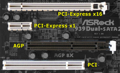
The PCI (Peripheral Component Interconnect) architecture was introduced by Intel in 1992, but did not gain significant traction over the established VESA Local Bus (VLB) in the consumer market until 1994. It was originally released only as a component specification, but later revisions added requirements for shape of connectors and motherboard slots. The bus supports both 32-bit and 4-bit bus widths. Four interrupt lines are shared by all devices on the bus, but are shifted by one position between devices so they are used evenly. For example, interrupt "A" on the first device is shifted to interrupt "B" on the second device, to interrupt "C" on the third device, and so on. The original specification provided a 33 MHz bus speed for a peak transfer rate of 133 MB/second for a 32-bit bus, and 266 MB/second for a 64-bit bus. Later revisions of the standard increased the frequency to 66 MHz, with a peak transfer rate of 533 MB/second for a 64-bit bus.
As time progressed, heavily-graphical applications (such as video games) began pushing the limits of the shared PCI bus. In response to this, the Accelerated Graphics Port (AGP) standard appeared in 1997, which provided a direct connection between the processor and a single graphics device. AGP is commonly referred to as a bus, but it is in fact a simple point-to-point channel. The single-purpose nature of this pathway allowed higher performance than could be attained when a graphics adapter shared the PCI bus. AGP was released in 1x, 2x, 4x, and 8x variants, which allowed data rates ranging from 266 MB/second up to 2133 MB/second. Higher data rates in later revisions were achieved with a constant clock speed of 66 MHz using double-data rate (DDR) and quad-data rate (QDR) techniques, among others.
In 1998, Compaq, IBM, and HP submitted a specification for PCI Extended (PCI-X) to the PCI Special Interest Group of the ACM, where it was ratified as an open standard. PCI-X doubled the bus speed over "traditional" PCI to 133 MHz, allowing for throughput up to 1.06 GB/second. This was needed because some devices, such as Gigabit ethernet cards, were saturating the PCI bus. Later revisions to PCI-X were ratified in 2003, and added even higher clock speeds (up to 533 MHz) and correspondingly higher throughputs. PCI-X never gained much market share, however, as hardware manufacturers largely chose to adopt PCI Express (PCI-E) instead.
Serial Buses
In 2001, the open HyperTransport specification was released by the HyperTransport Consortium. It provided bidirectional packet-based communications between components. It could be considered a "hybrid" technology, as it supports data widths from 2 bits (one in each direction) to 32 bits (16 in each direction). Communication frequencies are auto-negotiated between the devices up to 2.6 GHz, providing a maximum bandwidth of 20.8 GB/second in each direction. An extension called HyperTransport eXpansion (HTX) was developed which allows plug-in cards direct access to a CPU and system memory; this gives them the ability to act as "first class citizens" on the motherboard. Using this mechanism, companies have even developed their own devices (mostly FPGAs) which can be plugged directly into the CPU socket. HyperTransport technology has been deployed in a broad range of devices, from the Microsoft XBox gaming console to Cisco routers.
To replace the existing PCI, PCI-X, and AGP buses, Intel released the serial PCI Express (PCIe) in 2004. PCIe was designed to be software-compatible with existing PCI devices. Although the serial link transmits only one bit at a time, the specification allows up to 32 of these serial links (called "lanes") to be used concurrently. The lanes are not clock-synchronized; rather, the data are encoded using the 8b/10b scheme, which allows the receiver to automatically discover the clock from the data. They operate at 2.5 GHz, allowing for a maximum effective throughput at 32 lanes of 8 GB/second in each direction. Physically, PCIe devices are connected using a crossbar switch, which allows dynamic reallocation of communication lanes between any pair of devices. This is an improvement over the bus architectures, in which only one device could communicate at a time. Multiple lanes can be allocated between a pair of devices to achieve higher bandwidth communications. When multiple lanes are allocated to a given pair of devices, the data are interleaved across the lanes. This is referred to in the specification as "data striping". Version 2.0 of PCIe was released in January of 2007, which retains backward compatibility but allows for a doubling of the data rate in each of the lanes to 500 MB/second.
Conclusion
As mentioned in the beginning of this article, the main architectural trends are still the same: increasing logic density, exploiting instruction-level parallelism and multiprocessing. The only thing that changed is the scale on which ILP and TLP is happening. Ready access to high-density logic, high-speed buses and CPU interconnects, has provided an opportunity to mass-market systems with real parallel architecture for the first time. About 10 years ago NUMA (Non-Uniform Memory Access) systems were only talked about in context of supercomputers. Today anyone can afford a Dual-Socket AMD system that is a real NUMA machine, since each CPU has it's own memory controller, therefore making a distinction between "local" and "remote" memory.
References / Extra info
- http://www.intel.com/pressroom/archive/releases/20070128comp.htm
- http://www.intel.com/pressroom/archive/releases/20060125comp.htm
- http://domino.research.ibm.com/comm/pr.nsf/pages/news.20010425_Carbon_Nanotubes.html
Intel P6 Arch http://studies.ac.upc.edu/ETSETB/SEGPAR/microprocessors/pentium2%20(mpr).pdf
Intel Netburst http://en.wikipedia.org/wiki/NetBurst
Intel P4 microarch http://www.intel.com/technology/itj/q12001/pdf/art_2.pdf
Peripheral Component Interconnect (PCI) http://en.wikipedia.org/wiki/Peripheral_Component_Interconnect
Peripheral Component Interconnect Extended (PCI-X) http://en.wikipedia.org/wiki/PCI-X
Accelerated Graphics Port (AGP) http://en.wikipedia.org/wiki/Accelerated_Graphics_Port
HyperTransport http://en.wikipedia.org/wiki/HyperTransport
1 GHz HyperTransport Technology http://www.amd.com/us-en/Processors/ComputingSolutions/0,,30_288_13265_13295%5E13340,00.html
AMD K7 http://www.amd.com/us-en/assets/content_type/white_papers_and_tech_docs/22054.pdf
AMD K8 http://www.cpuid.com/reviews/K8/index.php
Aual and Single Core Opteron http://www-03.ibm.com/servers/eserver/opteron/pdf/IBM_dualcore_whitepaper.pdf
Intel Itanium http://en.wikipedia.org/wiki/Image:Itanium_arch.png
Sun Niagara http://www.opensparc.net/pubs/preszo/06/multicore/Niagara_Microarchitecture_ooox-Poonacha.pdf
IBM Cell http://domino.research.ibm.com/comm/research.nsf/pages/r.arch.innovation.html
NVidia GeForce 6 series http://download.nvidia.com/developer/GPU_Gems_2/GPU_Gems2_ch30.pdf
Radeon X 1800 http://www.hothardware.com/articles/ATI_X1000_Graphics_Family/?page=4