Chp8 my: Difference between revisions
(→AMD) |
|||
| (146 intermediate revisions by 3 users not shown) | |||
| Line 1: | Line 1: | ||
==Overview== | |||
We will introduce three different coherence protocols which are MSI, MESI and MOESI. Here we divide all material in several parts. | |||
*First, cache coherence: it includes the basic definition. | |||
*Second, MSI protocol: this section has the base introduction of MSI and how it works. | |||
*Third, MESI protocol: this section has the base information about MESI and we also introduce how Intel and AMD implements MESI in their processors. | |||
*Forth, MOESI protocol, this section has the base information about MOESI and we also introduce how AMD implements MOESI in their processors. | |||
*Last, MSI protocol is barely used by most companies, but we still found out that how to make MSI and MESI work together. Also, we will mention how MSI and MOESI, and MESI and MOESI protocols work together. We will have the comparison first and then also introduce how companies combine different coherence protocols in their processors or multiprocessors System-on-chips products. | |||
However, there are only a few theory about Firefly and Dragon protocols instead of implementation in real machine or processors. So, we only introduce how Intel and AMD implement MESI and MOESI in their processor products. | |||
==Cache Coherence== | ==Cache Coherence== | ||
In computing, cache coherence (also cache coherency) refers to the consistency of data stored in local caches of a shared resource. Cache coherence is a special case of memory coherence. | |||
===Definition=== | ===Definition=== | ||
In computing, cache coherence (also cache coherency) refers to the integrity of data stored in local caches of a shared resource. Cache coherence is a special case of memory coherence. In order to maintain the property of correct accesses to memory, system engineers develop kinds of coherence protocols to tackle them down. In this section, coherence protocols in bus-based multiprocessors are discussed.[1] | |||
The coherence of caches is obtained if the following conditions are met: | |||
# A read made by a processor P to a location X that follows a write by the same processor P to X, with no writes of X by another processor occurring between the write and the read instructions made by P, X must always return the value written by P. This condition is related with the program order preservation, and this must be achieved even in monoprocessed architectures. | |||
# A read made by a processor P1 to location X that follows a write by another processor P2 to X must return the written value made by P2 if no other writes to X made by any processor occur between the two accesses. This condition defines the concept of coherent view of memory. If processors can read the same old value after the write made by P2, we can say that the memory is incoherent. | |||
# Writes to the same location must be sequenced. In other words, if location X received two different values A and B, in this order, by any two processors, the processors can never read location X as B and then read it as A. The location X must be seen with values A and B in that order. | |||
'''Bus sniffing''' is the process where the individual caches monitor address lines for accesses to memory locations that they have cached. When a write operation is observed to a location that a cache has a copy of, the cache controller invalidates its own copy of the snooped memory location. | |||
'''System-on-a-chip (SOC)''': It refers to integrate all components of a computer or other electronic system into a single integrated circuit (chip). It may contain digital, analog, mixed-signal, and often radio-frequency functions – all on a single chip substrate. Mostly, it uses in embedded systems. | |||
==Coherency protocol== | ==Coherency protocol== | ||
[[Image:MOESI-sheet.jpg]] | |||
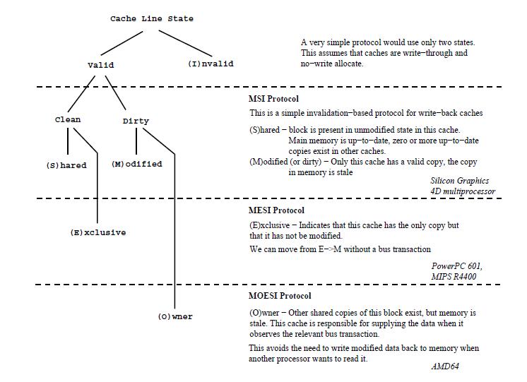
All the protocols talked about here are for write-back caches.[6] | |||
===MSI protocol=== | ===MSI protocol=== | ||
The simplest write back protocol is MSI protocol, therefore it is not deployed in real processors. Although it is not really in use, it is a good start to understand complicated protocols derived from this basic prototype.[14] | |||
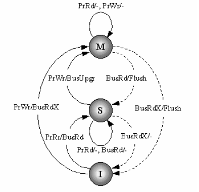
In MSI protocol, there are two processor requests and four bus side requests. | |||
*PrRd: processor side request to read to a cache block; | |||
*PrWr: processor side request to write to a cache block; | |||
*BusRd: snooped request that indicates there is a read request to a cache block made by another processor; | |||
*BusRdX: snooped request that indicates there is a write(read exclusive) request to a cache block made by another processor if that processor does not have a valid copy of the block; | |||
*BusUpgr: snooped request that indicates there is a write(read exclusive) request to a cache block made by another processor if that processor already has a valid copy of the block; | |||
*Flush: snooped request that indicates that an entire cache block is written back to the main memory by another processor; | |||
Each cache block has an associated state which could be one of the following three: | |||
*Modified(M): the cache block is valid in only one cache, and it implies exclusive ownership of the cache. Modifed state means both the cache is different from the value in the main memory, and it is cached only in one location. | |||
*Shared(S): the cache block is valid, and maybe shared by multiple processors. Shared also means the value is the same as the one in the main memory. | |||
*Invalid(I): the cache block is invalid. | |||
The state transition diagram for MSI protocol is showed below. | |||
[[Image:MSI.png]] | |||
===MESI protocol=== | ===MESI protocol === | ||
In MESI protocol, there are four cache block status: | ====MESI basics==== | ||
In MESI protocol, there are four cache block status[13]: | |||
*1. Modified (M): the cache block valid in only one cache and the value is like different from the main memory. | *1. Modified (M): the cache block valid in only one cache and the value is like different from the main memory. | ||
*2. Exclusive (E): the cache block is valid and clean, but only resides in one cache. | *2. Exclusive (E): the cache block is valid and clean, but only resides in one cache. | ||
*3. Shared (S): the cache block is valid and clean, but may exist in multiple caches. | *3. Shared (S): the cache block is valid and clean, but may exist in multiple caches. | ||
*4. Invalid (I): the cache block is invalid. | *4. Invalid (I): the cache block is invalid. | ||
Here we will introduce how Intel implements MESI. There are still four states, Modified, Exclusive, Shared and Invalid state.[2,9,10,11] | |||
In '''Modified''' state: | |||
Read request: it still keeps in Modified state and transfer the data to the CPU. | |||
Write request: it still keeps in Modified state and writes in the cache. | |||
Snooping result: cache line might write-back to main memory and changes states from Modified to Shared. Or, it might write-back | |||
to main memory and changes from Modified to Invalid. | |||
In '''Exclusive''' state: | |||
Read request: it still keeps in Exclusive state and transfer the data to the CPU. | |||
Write request: it will become Modified state and hold in the cache. | |||
Snooping result: it might changes to Shared or Invalid state. | |||
In '''Shared''' state: | |||
Read request: it will still in Shared state and transfers the data to the CPU. | |||
Write request: There are two situations might happen here. The first one is it goes to Exclusive state and being exclusive. The other one is to still keep Shared state with write-through cache and update data to the main memory. | |||
Snooping request: there will be transitions which are Shared or Invalid. | |||
In '''Valid''' state: | |||
Read request: There are three transitions might happen here. First of all, if the data read into to the cache, then it will become exclusive. Secondly, it might become Shared state after reading the data into the cache. Last, it will be still Invalid if there is a read/write miss happens. | |||
Write request: there will happen write miss and still in Invalid state. | |||
Snooping result: it will still go back to Invalid state, because the cache does have any data checked. | |||
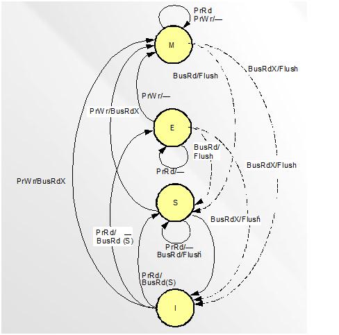
We are going to introduce those requests. | |||
*PrRd: processors request to read a cache block. | |||
*PrWr: processors request to write a cache block. | |||
*BusRd: snooped request a read request to a cache block made by another processor. | |||
*BusRdX: snooped request a read exclusive (write) request to a cache block made by another processor which doesn't already have the block. Shortly, write cache-to-memory | |||
*BusUpgr: snooped request indicates that there is a write request to a cache block that another processor already has in its cache. | |||
*Flush: snooped request indicates than an entire cache block is written back to main memory by another processors. | |||
*FlushOpt: snooped request indicates that an entire block cache block is posted on the bus in order to supply it to another processor. Shortly, cache-to-cache. | |||
| Line 28: | Line 99: | ||
This figure shows the status change when bus traction generated. | This figure shows the status change when bus traction generated. | ||
=== | ====Implement MESI in Intel and AMD==== | ||
=====MESI protocol in Dual-Core architecture===== | |||
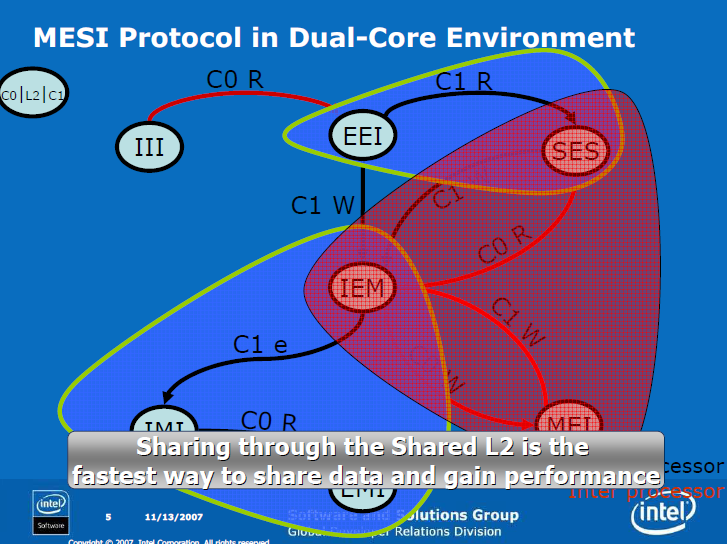
Cache-line states have two variations: core scope means state in L1 data cache; processor scope means state in L1 + L2 caches. Data shared by cores can be exclusively owned by the processor. Data can be Modified in L1 data cache and Exclusive in the L2. | |||
Only modified data is transferred from one core to another. Non-modified data that is missing in the L2 is fetched from memory. | |||
=====Effective Sharing===== | |||
*Two cores in the same processor load data from the same cache line | |||
**Cache line is brought only once from the memory to the L2 cache | |||
**Reduces bus utilization | |||
*One core produces data and the other core later consumes it | |||
**As long as the produced data chunks are bigger than the L1 data cache and smaller than the L2 cache | |||
**Produced data is evicted from the L1 data cache to the L2 cache | |||
**Consumed data is fetched from the L2 cache | |||
[[Image:MESI.png]] | |||
=====MESI protocol in AMD architecture===== | |||
AMD started using MESI protocol in their product, AMD-K6®-III processor. Its Super7™ compatible, 321-pin ceramic pin grid array (CPGA) package enables the processor to reduce time-to-market by leveraging today’s cost-effective, industry-standard infrastructure to deliver a superior-performing PC solution. In the end of this session, we will talk about how AMD uses writthorugh and write-back in AMD-K6-III processor.[16] | |||
The AMD-K6-III has two different level cache. | |||
*Level one: it's writeback and using 32-Kbyte instruction cache and a 32-Kbyte data cache with two-way set associativity. | |||
*Level two: it's 256 Kbytes and a unified, four-way setassociative cache. | |||
The cache line size is 32 bytes, and lines are fetched from external memory using an efficient pipelined burst transaction. | |||
In level one, instruction cache is filled with from level-two cache or from external memory. Also, each instruction byte is analyzed for instruction boundaries to each instruction byte. So, it makes the decoders are able to decode mutiple instructions simultaneously and efficiently. | |||
In the following figure, we can see that the processor cache design takes advantage of sectored organization. Each sector consists of 64 bytes configured as two 32-byte cache lines. The two cache lines of a sector share a common tag but have separate pairs of MESI (Modified, Exclusive, Shared, Invalid) bits that track the state of each cache line. | |||
[[Image:Amdcachesize.jpg]] | |||
Here, we have two tables as below. One of them is for read access and the other one is for write access. | |||
*Type: behaviors that include read or write. | |||
*Cache state before access: the state of cache before access. | |||
*Access type: what kinds access type is doing now. | |||
*Cache state after access: the state of cache after access. | |||
[[Image:Mesi_amd.jpg]] | |||
Let's see why we have to fill the cache-line. The processor performs a cache-line fill for any area of system memory defined as cacheable. If an area of system memory is not explicitly defined as uncacheable by the software or system logic, or implicitly treated as uncacheable by the processor, then the memory access is assumed to be cacheable. | |||
Now, lets' talk about cache misses and replaces. | |||
When a cache miss occurs in the L1 cache, the required cache line is filled from either the L2 cache, if the cache line is present (L2 cache hit), or from external memory, if the cache line is not present (L2 cache miss). If the cache line is filled from external memory, the cache line is filled in both the L1 and the L2 caches. Furthermore, here we are going to introduce another two forms of cache misses and associated cache fills can take place a write/read-miss cache fill and a write/read-hit cache fill. In the case of a write/read-miss cache fill, the level-one cache miss is due to a write/read | |||
mismatch, in which case the required cache line is filled either from the level-two cache or from external memory, and the level-one cache line within the sector that was not required is marked as invalid. In the case of a write/read-hit cache fill, the address matches the tag, but the requested cache line is marked as invalid. The required level-one cache line is filled from the level-two cache or from external memory, and the level-one cache line within the sector that is not required remains in the | |||
same cache state. | |||
If a L1 data-cache line being filled replaces a modified line, the modified line is written back to the L2 cache if the cache line is present (L2 cache hit). By design, if a cache line is in the modified state in the L1 cache, this cache line can only exist in the L2 cache in the exclusive state. During the writeback, the L2 cache-line state is changed from exclusive to modified, and | |||
the writeback does not occur on the system bus. If the replacement writeback does not hit the L2 cache (L2 cache miss), then the modified L1 cache line is written back on the system bus, and the L2 cache is not updated. If the other cache | |||
line in this sector is in the modified state, it is also written back in the same manner. | |||
The below figure presents us how snooper works in MESI protocol in AMD-K6-III processor. | |||
[[Image:Snooper_mesi_amd.jpg]] | |||
This snooper figure works as well as MESI bus figure which we mention previously. It shows all possible states when there is a behavior generated. It might flush to all the memory or just cache-to-cache transfer. | |||
AMD applies write-through and write-back in AMD-K6-III processor. Here, we will explain how they use both of them in AMD-K6-III processor. | |||
*Write-through: (1)An external memory write that occurs concurrently with a cache update to the same location. (2)Shared and invalid MESI lines are in the writethrough state. | |||
*Write-back: (1) An external memory write that occurs after the processor has modified a cache line. (2) Modified and exclusive MESI lines are in the writeback state. | |||
==== | ===MOESI protocol (AMD)=== | ||
====MOESI basics==== | |||
AMD Opteron is using MOESI (modified, owned, exclusive, shared, invalid) protocol for cache sharing. In addition to the four states in MESI, which is adopted by Intel for their Xeon processors, a fifth state "Owned" appears here representing data that is both modified and shared. Using MOESI, writing modified data back to main memory is avoided before being shared, which could save bandwidth and gain much faster access to users to the cache. | AMD Opteron is using MOESI (modified, owned, exclusive, shared, invalid) protocol for cache sharing. In addition to the four states in MESI, which is adopted by Intel for their Xeon processors, a fifth state "Owned" appears here representing data that is both modified and shared. Using MOESI, writing modified data back to main memory is avoided before being shared, which could save bandwidth and gain much faster access to users to the cache. | ||
| Line 56: | Line 188: | ||
correct data. Unlike the shared state, however, the copy in main memory can be stale (incorrect). | correct data. Unlike the shared state, however, the copy in main memory can be stale (incorrect). | ||
Only one processor can hold the data in the owned state—all other processors must hold the data in | Only one processor can hold the data in the owned state—all other processors must hold the data in | ||
the shared state.</li> | the shared state.</li></ul> | ||
</ | |||
The first figure below shows the five different states of MOESI protocol. There are four valid states: M(odified) and E(xclusive) are not shared with other cache, while O(wned) and S(hared) with other caches. The second figure shows the state transitions of MOESI protocol. | |||
[[Image:Opteron moesi.gif]][[Image:Moesi.png]] | |||
====AMD Special Coherency Considerations==== | |||
In some cases, data can be modified in a manner that is impossible for the memory-coherency protocol to handle due to the effects of instruction prefetching. In such situations software must use serializing | |||
instructions and/or cache-invalidation instructions to guarantee subsequent data accesses are coherent. An example of this type of a situation is a page-table update followed by accesses to the physical pages | |||
referenced by the updated page tables. The following sequence of events shows what can happen when software changes the translation of virtual-page A from physical-page M to physical-page N: | |||
<ol> | |||
<li>Software invalidates the TLB entry. The tables that translate virtual-page A to physical-page M are now held only in main memory. They are not cached by the TLB.</li> | |||
<li>Software changes the page-table entry for virtual-page A in main memory to point to physicalpage N rather than physical-page M.</li> | |||
<li>Software accesses data in virtual-page A. During Step 3, software expects the processor to access the data from physical-page N. However, it is possible for the processor to prefetch the data from physical-page M before the page table for virtualpage A is updated in Step 2. This is because the physical-memory references for the page tables are different than the physical-memory references for the data. Because the physical-memory references are different, the processor does not recognize them as requiring coherency checking and believes it is safe to prefetch the data from virtual-page A, which is translated into a read from physical page M. Similar behavior can occur when instructions are prefetched from beyond the page table update instruction.</li> | |||
</ol> | |||
To prevent this problem, software must use an INVLPG or MOV CR3 instruction immediately after the page-table update to ensure that subsequent instruction fetches and data accesses use the correct virtual-page-to-physical-page translation. It is not necessary to perform a TLB invalidation operation preceding the table update. | |||
==Cache Coherence Protocol Comparision== | |||
We are going to introduce the difference between MOESI and MESI protocols. Here we put a chart to show the difference among them. | |||
[[Image:MOESI_MESI.jpg]] | |||
The snoop request always happens as a read or write request. When a processor has a write request, it will invalid other processors and asks them to evict the cache line. The two protocols used for x86 microprocessors are MESI (Intel: x86 and IPF) and MOESI (AMD). MESI is a two hop protocol and every cache line is held in one of four states, which track meta data, such as whether the data is shared or has been modified. | |||
In contrast, MOESI is a three hop protocol with slightly modified states. Under MOESI, a processor can write to a line in the cache, and then put it in the O state and share the data, without writing the cache line back to memory (i.e. it allows for sharing dirty data). This can be advantageous, particularly for multi-core processors that do not share the last level of cache. For the MESI protocol, this would require an additional write back to main memory<ref>15</ref>. | |||
==Combination== | |||
===MSI and MESI=== | |||
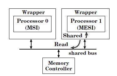
We will talk about how to combine MSI and MESI protocols together. | |||
[[Image:Msiandmesisharebus.jpg]] | |||
MESI protocol has one more state, which is Exclusive state, than MSI protocol. The E state is not allowed in integrating MSI and | |||
MESI protocols. Using the MESI protocol as an example, the I→E transition occurs only when a processor initiates a read transaction on the bus, and other processors on the system do not have the same block in their caches. The sharing information is delivered by the shared signal. | |||
Therefore, the technique to remove the E state is to assert the shared signal within the processor’s wrapper, whenever a memory read transaction is initiated by its own processor. Like the read-to-write conversion, | |||
it can be implemented within the wrappers, as shown in the above figure. With this technique, the operation (b) invokes the I→S state transition in P1, and the operation (d) makes the M→S transition in P1, resulting in coherent caches. In the following figure displays the difference between with this solution (remove E) and without this solution. | |||
[[Image:msiandmesi.jpg]] | |||
Implementation cost: The implementation of the shared signal assertion requires asserting the shared signal to its own processor whenever a read miss occurs. | |||
=== | ===MESI & MOESI, and MSI & MOESI=== | ||
We will discuss how to combine "MESI and MOESI" & "MSI and MOESI" together, because the way to combine is very similar. | |||
This combination prohibits the E state to avoid the problem, which E only appears a small portion of the whole transition, in the following table. | |||
We employ the shared signal assertion to remove the E state. The transition to the | |||
O state is permitted as long as the cache coherence-enforced memory controller (ccMC) has the discretion to differentiate the O and | |||
S states. As a result, the integrated protocol becomes equivalent to MSI with the O | |||
state enabled[17]. | |||
[[Image:Msiandmoesi.jpg]] | |||
This table explains two things. The first one is without shared signal assertion and the second one is applying shared signal assertion. If we don't have shared signal assertion, them we would not be able to remove E state. If we do have share signal assertion, then we will remove E state and reduce any occasion that happens E state. | |||
==References== | ==References== | ||
| Line 72: | Line 252: | ||
<li>[http://www.zak.ict.pwr.wroc.pl/nikodem/ak_materialy/Cache%20consistency%20&%20MESI.pdf Cache consistency & MESI Intel]</li> | <li>[http://www.zak.ict.pwr.wroc.pl/nikodem/ak_materialy/Cache%20consistency%20&%20MESI.pdf Cache consistency & MESI Intel]</li> | ||
<li>[http://techreport.com/articles.x/8236/2 A closer look at AMD's dual-core architecture]</li> | <li>[http://techreport.com/articles.x/8236/2 A closer look at AMD's dual-core architecture]</li> | ||
<li>[http://www.csd.uoc.gr/~poisson/courses/CSD-527-report-engl.pdf Trace-Driven Simulation of the MSI, MESI and Dragon Cache Coherence Protocols]</li> | <li>[http://www.csd.uoc.gr/~poisson/courses/CSD-527-report-engl.pdf Trace-Driven Simulation of the MSI, MESI and Dragon Cache Coherence Protocols]</li> | ||
<li>[http://www.chip-architect.com/news/2003_09_21_Detailed_Architecture_of_AMDs_64bit_Core.html Understanding the Detailed Architecture of AMD's 64 bit Core]</li> | <li>[http://www.chip-architect.com/news/2003_09_21_Detailed_Architecture_of_AMDs_64bit_Core.html Understanding the Detailed Architecture of AMD's 64 bit Core]</li> | ||
<li>[http://www.wiki.cl.cam.ac.uk/rowiki/CompArch/ACS-CMP/Seminar4 MSI,MESI,MOESI sheet]</li> | <li>[http://www.wiki.cl.cam.ac.uk/rowiki/CompArch/ACS-CMP/Seminar4 MSI,MESI,MOESI sheet]</li> | ||
<li>[http://www.amd.com/us-en/assets/content_type/white_papers_and_tech_docs/24593.pdf AMD64 Architecture Programmer’s Manual]</li> | |||
<li>[ftp://download.intel.com/design/pentium/datashts/24199710.pdf Intel PENTIUM]</li> | |||
<li>[ftp://download.intel.com/design/intarch/manuals/27320401.pdf Intel Corporation (1998). “Embedded Pentium Processor Family Developer’s Manual.”]</li> | |||
<li>[ftp://download.intel.com/design/PentiumII/manuals/24319002.pdf Intel Corporation (2002).Intel Architecture Software Developer's Manual, Volume 1:basic Architecture]</li> | |||
<li>[ftp://download.intel.com/design/intarch/papers/cache6.pdf Intel Corporation (2002). “An Overview of Cache]</li> | |||
<li>[ftp://download.intel.com/design/intarch/manuals/27320401.pdf Embedded Pentium® Processor Family]</li> | |||
<li>[http://www.csc.ncsu.edu/faculty/efg/506/s10/ NCSU CSC 506 Parallel Computing Systems]</li> | |||
<li>Fundamentals of Parallel Computer Archiecture by Yan Solihin</li> | |||
<li>[http://www.realworldtech.com/page.cfm?ArticleID=RWT121106171654&p=4 An Introduction to Multiprocessor Systems]</li> | |||
<li>[http://www.amd.com/us-en/assets/content_type/white_papers_and_tech_docs/21918.pdf AMD-K6-III Processor Data Sheet]</li> | |||
<li>[http://arch.ece.gatech.edu/pub/tsuh.pdf INTEGRATION AND EVALUATION OF CACHE COHERENCE PROTOCOLS FOR MULTIPROCESSOR SOCS]</li> | |||
</ol> | </ol> | ||
Latest revision as of 19:55, 4 May 2010
Overview
We will introduce three different coherence protocols which are MSI, MESI and MOESI. Here we divide all material in several parts.
- First, cache coherence: it includes the basic definition.
- Second, MSI protocol: this section has the base introduction of MSI and how it works.
- Third, MESI protocol: this section has the base information about MESI and we also introduce how Intel and AMD implements MESI in their processors.
- Forth, MOESI protocol, this section has the base information about MOESI and we also introduce how AMD implements MOESI in their processors.
- Last, MSI protocol is barely used by most companies, but we still found out that how to make MSI and MESI work together. Also, we will mention how MSI and MOESI, and MESI and MOESI protocols work together. We will have the comparison first and then also introduce how companies combine different coherence protocols in their processors or multiprocessors System-on-chips products.
However, there are only a few theory about Firefly and Dragon protocols instead of implementation in real machine or processors. So, we only introduce how Intel and AMD implement MESI and MOESI in their processor products.
Cache Coherence
In computing, cache coherence (also cache coherency) refers to the consistency of data stored in local caches of a shared resource. Cache coherence is a special case of memory coherence.
Definition
In computing, cache coherence (also cache coherency) refers to the integrity of data stored in local caches of a shared resource. Cache coherence is a special case of memory coherence. In order to maintain the property of correct accesses to memory, system engineers develop kinds of coherence protocols to tackle them down. In this section, coherence protocols in bus-based multiprocessors are discussed.[1]
The coherence of caches is obtained if the following conditions are met:
- A read made by a processor P to a location X that follows a write by the same processor P to X, with no writes of X by another processor occurring between the write and the read instructions made by P, X must always return the value written by P. This condition is related with the program order preservation, and this must be achieved even in monoprocessed architectures.
- A read made by a processor P1 to location X that follows a write by another processor P2 to X must return the written value made by P2 if no other writes to X made by any processor occur between the two accesses. This condition defines the concept of coherent view of memory. If processors can read the same old value after the write made by P2, we can say that the memory is incoherent.
- Writes to the same location must be sequenced. In other words, if location X received two different values A and B, in this order, by any two processors, the processors can never read location X as B and then read it as A. The location X must be seen with values A and B in that order.
Bus sniffing is the process where the individual caches monitor address lines for accesses to memory locations that they have cached. When a write operation is observed to a location that a cache has a copy of, the cache controller invalidates its own copy of the snooped memory location.
System-on-a-chip (SOC): It refers to integrate all components of a computer or other electronic system into a single integrated circuit (chip). It may contain digital, analog, mixed-signal, and often radio-frequency functions – all on a single chip substrate. Mostly, it uses in embedded systems.
Coherency protocol
All the protocols talked about here are for write-back caches.[6]
MSI protocol
The simplest write back protocol is MSI protocol, therefore it is not deployed in real processors. Although it is not really in use, it is a good start to understand complicated protocols derived from this basic prototype.[14]
In MSI protocol, there are two processor requests and four bus side requests.
- PrRd: processor side request to read to a cache block;
- PrWr: processor side request to write to a cache block;
- BusRd: snooped request that indicates there is a read request to a cache block made by another processor;
- BusRdX: snooped request that indicates there is a write(read exclusive) request to a cache block made by another processor if that processor does not have a valid copy of the block;
- BusUpgr: snooped request that indicates there is a write(read exclusive) request to a cache block made by another processor if that processor already has a valid copy of the block;
- Flush: snooped request that indicates that an entire cache block is written back to the main memory by another processor;
Each cache block has an associated state which could be one of the following three:
- Modified(M): the cache block is valid in only one cache, and it implies exclusive ownership of the cache. Modifed state means both the cache is different from the value in the main memory, and it is cached only in one location.
- Shared(S): the cache block is valid, and maybe shared by multiple processors. Shared also means the value is the same as the one in the main memory.
- Invalid(I): the cache block is invalid.
The state transition diagram for MSI protocol is showed below.
MESI protocol
MESI basics
In MESI protocol, there are four cache block status[13]:
- 1. Modified (M): the cache block valid in only one cache and the value is like different from the main memory.
- 2. Exclusive (E): the cache block is valid and clean, but only resides in one cache.
- 3. Shared (S): the cache block is valid and clean, but may exist in multiple caches.
- 4. Invalid (I): the cache block is invalid.
Here we will introduce how Intel implements MESI. There are still four states, Modified, Exclusive, Shared and Invalid state.[2,9,10,11]
In Modified state:
Read request: it still keeps in Modified state and transfer the data to the CPU.
Write request: it still keeps in Modified state and writes in the cache.
Snooping result: cache line might write-back to main memory and changes states from Modified to Shared. Or, it might write-back
to main memory and changes from Modified to Invalid.
In Exclusive state:
Read request: it still keeps in Exclusive state and transfer the data to the CPU.
Write request: it will become Modified state and hold in the cache.
Snooping result: it might changes to Shared or Invalid state.
In Shared state:
Read request: it will still in Shared state and transfers the data to the CPU.
Write request: There are two situations might happen here. The first one is it goes to Exclusive state and being exclusive. The  other one is to still keep Shared state with write-through cache and update data to the main memory.
Snooping request: there will be transitions which are Shared or Invalid.
In Valid state:
Read request: There are three transitions might happen here. First of all, if the data read into to the cache, then it will become exclusive. Secondly, it might become Shared state after reading the data into the cache. Last, it will be still Invalid if there is a read/write miss happens.
Write request: there will happen write miss and still in Invalid state.
Snooping result: it will still go back to Invalid state, because the cache does have any data checked.
We are going to introduce those requests.
- PrRd: processors request to read a cache block.
- PrWr: processors request to write a cache block.
- BusRd: snooped request a read request to a cache block made by another processor.
- BusRdX: snooped request a read exclusive (write) request to a cache block made by another processor which doesn't already have the block. Shortly, write cache-to-memory
- BusUpgr: snooped request indicates that there is a write request to a cache block that another processor already has in its cache.
- Flush: snooped request indicates than an entire cache block is written back to main memory by another processors.
- FlushOpt: snooped request indicates that an entire block cache block is posted on the bus in order to supply it to another processor. Shortly, cache-to-cache.
This figure shows the status change when bus traction generated.
Implement MESI in Intel and AMD
MESI protocol in Dual-Core architecture
Cache-line states have two variations: core scope means state in L1 data cache; processor scope means state in L1 + L2 caches. Data shared by cores can be exclusively owned by the processor. Data can be Modified in L1 data cache and Exclusive in the L2.
Only modified data is transferred from one core to another. Non-modified data that is missing in the L2 is fetched from memory.
Effective Sharing
- Two cores in the same processor load data from the same cache line
- Cache line is brought only once from the memory to the L2 cache
- Reduces bus utilization
- One core produces data and the other core later consumes it
- As long as the produced data chunks are bigger than the L1 data cache and smaller than the L2 cache
- Produced data is evicted from the L1 data cache to the L2 cache
- Consumed data is fetched from the L2 cache
MESI protocol in AMD architecture
AMD started using MESI protocol in their product, AMD-K6®-III processor. Its Super7™ compatible, 321-pin ceramic pin grid array (CPGA) package enables the processor to reduce time-to-market by leveraging today’s cost-effective, industry-standard infrastructure to deliver a superior-performing PC solution. In the end of this session, we will talk about how AMD uses writthorugh and write-back in AMD-K6-III processor.[16]
The AMD-K6-III has two different level cache.
- Level one: it's writeback and using 32-Kbyte instruction cache and a 32-Kbyte data cache with two-way set associativity.
- Level two: it's 256 Kbytes and a unified, four-way setassociative cache.
The cache line size is 32 bytes, and lines are fetched from external memory using an efficient pipelined burst transaction. In level one, instruction cache is filled with from level-two cache or from external memory. Also, each instruction byte is analyzed for instruction boundaries to each instruction byte. So, it makes the decoders are able to decode mutiple instructions simultaneously and efficiently.
In the following figure, we can see that the processor cache design takes advantage of sectored organization. Each sector consists of 64 bytes configured as two 32-byte cache lines. The two cache lines of a sector share a common tag but have separate pairs of MESI (Modified, Exclusive, Shared, Invalid) bits that track the state of each cache line.
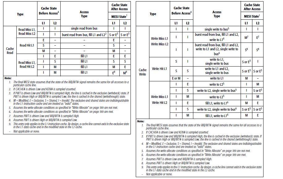
Here, we have two tables as below. One of them is for read access and the other one is for write access.
- Type: behaviors that include read or write.
- Cache state before access: the state of cache before access.
- Access type: what kinds access type is doing now.
- Cache state after access: the state of cache after access.
Let's see why we have to fill the cache-line. The processor performs a cache-line fill for any area of system memory defined as cacheable. If an area of system memory is not explicitly defined as uncacheable by the software or system logic, or implicitly treated as uncacheable by the processor, then the memory access is assumed to be cacheable.
Now, lets' talk about cache misses and replaces.
When a cache miss occurs in the L1 cache, the required cache line is filled from either the L2 cache, if the cache line is present (L2 cache hit), or from external memory, if the cache line is not present (L2 cache miss). If the cache line is filled from external memory, the cache line is filled in both the L1 and the L2 caches. Furthermore, here we are going to introduce another two forms of cache misses and associated cache fills can take place a write/read-miss cache fill and a write/read-hit cache fill. In the case of a write/read-miss cache fill, the level-one cache miss is due to a write/read mismatch, in which case the required cache line is filled either from the level-two cache or from external memory, and the level-one cache line within the sector that was not required is marked as invalid. In the case of a write/read-hit cache fill, the address matches the tag, but the requested cache line is marked as invalid. The required level-one cache line is filled from the level-two cache or from external memory, and the level-one cache line within the sector that is not required remains in the same cache state.
If a L1 data-cache line being filled replaces a modified line, the modified line is written back to the L2 cache if the cache line is present (L2 cache hit). By design, if a cache line is in the modified state in the L1 cache, this cache line can only exist in the L2 cache in the exclusive state. During the writeback, the L2 cache-line state is changed from exclusive to modified, and the writeback does not occur on the system bus. If the replacement writeback does not hit the L2 cache (L2 cache miss), then the modified L1 cache line is written back on the system bus, and the L2 cache is not updated. If the other cache line in this sector is in the modified state, it is also written back in the same manner.
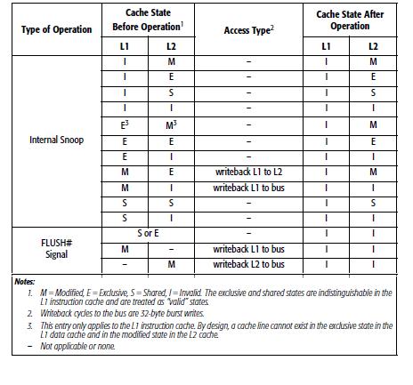
The below figure presents us how snooper works in MESI protocol in AMD-K6-III processor.
This snooper figure works as well as MESI bus figure which we mention previously. It shows all possible states when there is a behavior generated. It might flush to all the memory or just cache-to-cache transfer.
AMD applies write-through and write-back in AMD-K6-III processor. Here, we will explain how they use both of them in AMD-K6-III processor.
- Write-through: (1)An external memory write that occurs concurrently with a cache update to the same location. (2)Shared and invalid MESI lines are in the writethrough state.
- Write-back: (1) An external memory write that occurs after the processor has modified a cache line. (2) Modified and exclusive MESI lines are in the writeback state.
MOESI protocol (AMD)
MOESI basics
AMD Opteron is using MOESI (modified, owned, exclusive, shared, invalid) protocol for cache sharing. In addition to the four states in MESI, which is adopted by Intel for their Xeon processors, a fifth state "Owned" appears here representing data that is both modified and shared. Using MOESI, writing modified data back to main memory is avoided before being shared, which could save bandwidth and gain much faster access to users to the cache.
The states of the MOESI protocol are:
- Invalid—A cache line in the invalid state does not hold a valid copy of the data. Valid copies of the data can be either in main memory or another processor cache.
- Exclusive—A cache line in the exclusive state holds the most recent, correct copy of the data. The copy in main memory is also the most recent, correct copy of the data. No other processor holds a copy of the data.
- Shared—A cache line in the shared state holds the most recent, correct copy of the data. Other processors in the system may hold copies of the data in the shared state, as well. If no other processor holds it in the owned state, then the copy in main memory is also the most recent.
- Modified—A cache line in the modified state holds the most recent, correct copy of the data. The copy in main memory is stale (incorrect), and no other processor holds a copy.
- Owned—A cache line in the owned state holds the most recent, correct copy of the data. The owned state is similar to the shared state in that other processors can hold a copy of the most recent, correct data. Unlike the shared state, however, the copy in main memory can be stale (incorrect). Only one processor can hold the data in the owned state—all other processors must hold the data in the shared state.
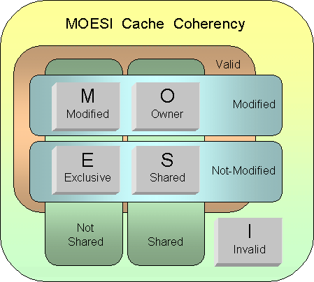
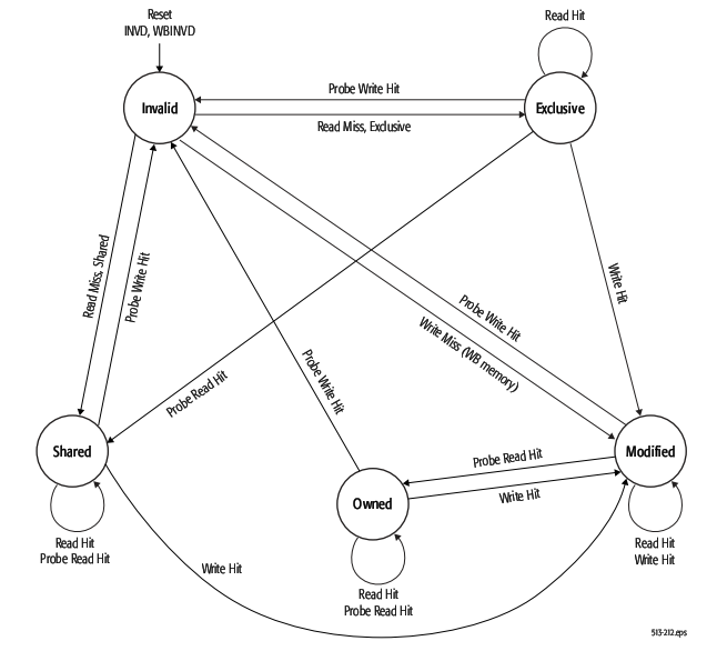
The first figure below shows the five different states of MOESI protocol. There are four valid states: M(odified) and E(xclusive) are not shared with other cache, while O(wned) and S(hared) with other caches. The second figure shows the state transitions of MOESI protocol.
AMD Special Coherency Considerations
In some cases, data can be modified in a manner that is impossible for the memory-coherency protocol to handle due to the effects of instruction prefetching. In such situations software must use serializing instructions and/or cache-invalidation instructions to guarantee subsequent data accesses are coherent. An example of this type of a situation is a page-table update followed by accesses to the physical pages referenced by the updated page tables. The following sequence of events shows what can happen when software changes the translation of virtual-page A from physical-page M to physical-page N:
- Software invalidates the TLB entry. The tables that translate virtual-page A to physical-page M are now held only in main memory. They are not cached by the TLB.
- Software changes the page-table entry for virtual-page A in main memory to point to physicalpage N rather than physical-page M.
- Software accesses data in virtual-page A. During Step 3, software expects the processor to access the data from physical-page N. However, it is possible for the processor to prefetch the data from physical-page M before the page table for virtualpage A is updated in Step 2. This is because the physical-memory references for the page tables are different than the physical-memory references for the data. Because the physical-memory references are different, the processor does not recognize them as requiring coherency checking and believes it is safe to prefetch the data from virtual-page A, which is translated into a read from physical page M. Similar behavior can occur when instructions are prefetched from beyond the page table update instruction.
To prevent this problem, software must use an INVLPG or MOV CR3 instruction immediately after the page-table update to ensure that subsequent instruction fetches and data accesses use the correct virtual-page-to-physical-page translation. It is not necessary to perform a TLB invalidation operation preceding the table update.
Cache Coherence Protocol Comparision
We are going to introduce the difference between MOESI and MESI protocols. Here we put a chart to show the difference among them.

The snoop request always happens as a read or write request. When a processor has a write request, it will invalid other processors and asks them to evict the cache line. The two protocols used for x86 microprocessors are MESI (Intel: x86 and IPF) and MOESI (AMD). MESI is a two hop protocol and every cache line is held in one of four states, which track meta data, such as whether the data is shared or has been modified.
In contrast, MOESI is a three hop protocol with slightly modified states. Under MOESI, a processor can write to a line in the cache, and then put it in the O state and share the data, without writing the cache line back to memory (i.e. it allows for sharing dirty data). This can be advantageous, particularly for multi-core processors that do not share the last level of cache. For the MESI protocol, this would require an additional write back to main memory<ref>15</ref>.
Combination
MSI and MESI
We will talk about how to combine MSI and MESI protocols together.
MESI protocol has one more state, which is Exclusive state, than MSI protocol. The E state is not allowed in integrating MSI and MESI protocols. Using the MESI protocol as an example, the I→E transition occurs only when a processor initiates a read transaction on the bus, and other processors on the system do not have the same block in their caches. The sharing information is delivered by the shared signal.
Therefore, the technique to remove the E state is to assert the shared signal within the processor’s wrapper, whenever a memory read transaction is initiated by its own processor. Like the read-to-write conversion,
it can be implemented within the wrappers, as shown in the above figure. With this technique, the operation (b) invokes the I→S state transition in P1, and the operation (d) makes the M→S transition in P1, resulting in coherent caches. In the following figure displays the difference between with this solution (remove E) and without this solution.
Implementation cost: The implementation of the shared signal assertion requires asserting the shared signal to its own processor whenever a read miss occurs.
MESI & MOESI, and MSI & MOESI
We will discuss how to combine "MESI and MOESI" & "MSI and MOESI" together, because the way to combine is very similar. This combination prohibits the E state to avoid the problem, which E only appears a small portion of the whole transition, in the following table. We employ the shared signal assertion to remove the E state. The transition to the O state is permitted as long as the cache coherence-enforced memory controller (ccMC) has the discretion to differentiate the O and S states. As a result, the integrated protocol becomes equivalent to MSI with the O state enabled[17].
This table explains two things. The first one is without shared signal assertion and the second one is applying shared signal assertion. If we don't have shared signal assertion, them we would not be able to remove E state. If we do have share signal assertion, then we will remove E state and reduce any occasion that happens E state.
References
- Cache Coherence
- Cache consistency & MESI Intel
- A closer look at AMD's dual-core architecture
- Trace-Driven Simulation of the MSI, MESI and Dragon Cache Coherence Protocols
- Understanding the Detailed Architecture of AMD's 64 bit Core
- MSI,MESI,MOESI sheet
- AMD64 Architecture Programmer’s Manual
- Intel PENTIUM
- Intel Corporation (1998). “Embedded Pentium Processor Family Developer’s Manual.”
- Intel Corporation (2002).Intel Architecture Software Developer's Manual, Volume 1:basic Architecture
- Intel Corporation (2002). “An Overview of Cache
- Embedded Pentium® Processor Family
- NCSU CSC 506 Parallel Computing Systems
- Fundamentals of Parallel Computer Archiecture by Yan Solihin
- An Introduction to Multiprocessor Systems
- AMD-K6-III Processor Data Sheet
- INTEGRATION AND EVALUATION OF CACHE COHERENCE PROTOCOLS FOR MULTIPROCESSOR SOCS
