CSC/ECE 506 Fall 2007/wiki1 7 a1: Difference between revisions
No edit summary |
|||
| (59 intermediate revisions by the same user not shown) | |||
| Line 1: | Line 1: | ||
Shared address space is an important class of the multiprocessors where all processors share a global memory. Communication between tasks running on different processors is performed through writing to and reading from the global memory. All interprocessor coordination and synchronization is also accomplished via the global memory. Hence, a shared memory computer system consists of a set of independent processors, a set of memory modules, and an interconnection network. | |||
This article talks about the recent trends in shared address space and how the interconnection technology has changed in last 10 years. Later it highlights some of the existing SMPs and latest supercomputer. | |||
==Recent Design Trends in Shared Address Space== | |||
Current high-performance multiprocessor platforms may be broken into two categories: distributed address-space and shared address-space. For programs running on a distributed address-space multiprocessor, data visible on one processing unit is not visible on the remaining processor units. In contrast, hardware mechanisms in high performance shared address-space environments ensure that all data is in principle visible to all processors. While a shared address-space can offer programmability advantages and better performance for fine-grained applications, the very mechanisms that create those advantages appear to prevent the machines from scaling to large numbers of processors. | |||
To scale beyond the limits of traditional shared address space architectures, hybrids of shared and distributed architectures are becoming more prevalent. These architectures allow users to take advantage of two or more address spaces to gain the scalability of distributed architectures while retaining the benefits of the shared address-space architecture. | |||
Memory is split into global, which hardware keeps coherent, and strictly local, which is left incoherent. Application programmers are given a mechanism for specifying, at a very high level, data that would benefit from localization – being moved from global to local memory. This transparency in memory partitioning takes place through improved compiler allocation mechanisms than the traditional hardware devices. The following are benefits of localizing otherwise remote memory accesses. | |||
1. Faster access to localized data. | |||
2. Elimination of redundant protocol traffic. | |||
3. Elimination of locking/contention for written shared data. | |||
A trend in application design is the use of vector instructions. This allows programs to deliver more fine grain tasks which capitalize on the parallel processing nature of a shared address space architecture. Vector instructions, also known as SIMD (single intruction multiple data), have been optimized on a series of recent architectures including the cell processor in Toshiba/Sony's PlayStation 3 game console. The PS3 cell processor consists of one scalar and eight vector processors. | |||
==Evolution of Interconnect Technology== | |||
The effectiveness of the shared memory approach depends on the latency incurred on the memory access as well as the bandwidth of the data transfer that can be supported. The interconnection network in a shared-memory multiprocessor has evolved over a decade to provide better aggregate bandwidth when more processors are added without increasing cost too much. | The effectiveness of the shared memory approach depends on the latency incurred on the memory access as well as the bandwidth of the data transfer that can be supported. The interconnection network in a shared-memory multiprocessor has evolved over a decade to provide better aggregate bandwidth when more processors are added without increasing cost too much. | ||
| Line 11: | Line 24: | ||
The single shared bus system has been extended to multiple buses to connect multiple processors. | The single shared bus system has been extended to multiple buses to connect multiple processors. | ||
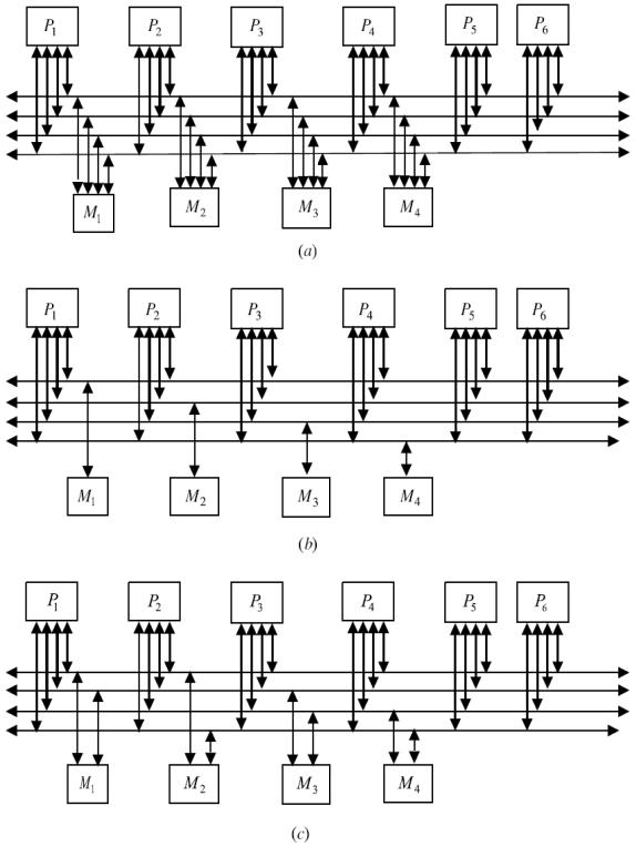
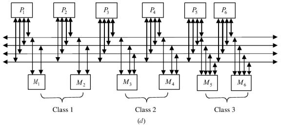
A multiple bus multiprocessor system uses several parallel buses to interconnect multiple processors and multiple memory modules. A number of connection schemes are possible in this case. Among the possibilities are the multiple bus with full bus–memory connection (MBFBMC), multiple bus with single bus memory connection (MBSBMC), multiple bus with partial bus–memory connection (MBPBMC), and multiple bus with class-based memory connection (MBCBMC). The multiple bus with full bus–memory connection has all memory modules connected to all buses. The multiple bus with single bus–memory connection has each memory module connected to a specific bus. The multiple bus with partial bus–memory connection has each memory module connected to a subset of buses. The multiple bus with class-based memory connection has memory modules grouped into classes whereby each class is connected to a specific subset of buses. A class is just an arbitrary collection of memory modules. | A multiple bus multiprocessor system uses several parallel buses to interconnect multiple processors and multiple memory modules. A number of connection schemes are possible in this case. Among the possibilities are the multiple bus with full bus–memory connection (MBFBMC), multiple bus with single bus memory connection (MBSBMC), multiple bus with partial bus–memory connection (MBPBMC), and multiple bus with class-based memory connection (MBCBMC). The multiple bus with full bus–memory connection has all memory modules connected to all buses. The multiple bus with single bus–memory connection has each memory module connected to a specific bus. The multiple bus with partial bus–memory connection has each memory module connected to a subset of buses. The multiple bus with class-based memory connection has memory modules grouped into classes whereby each class is connected to a specific subset of buses. A class is just an arbitrary collection of memory modules. Example of different multiple bus scheme for for the case of N = 6 processors, M = 4 memory modules, and B = 4 buses has been illustrated in the figure below. | ||
[[Image:Bus01.JPG]] | |||
[[Image:Bus02.JPG]] | |||
Figure 2.1 (a) Multiple bus with full bus–memory connection (MBFBMC); (b) multiple bus with single bus-memory connection (MBSBMC); (c) multiple bus with partial bus–memory connection (MBPBMC); and (d) multiple bus with class-based memory | |||
connection (MBCBMC). [Source: Reference 8] | |||
A typical bus-based design uses caches to solve the bus contention problem. Highspeed caches connected to each processor on one side and the bus on the other side mean that local copies of instructions and data can be supplied at the highest possible rate. If the local processor finds all of its instructions and data in the local cache, we say the hit rate is 100%. The miss rate of a cache is the fraction of the references that are not stored locally. The required data must be copied from the global memory, across the bus and into the cache. From there it is routed to the local processor. One of the goals of the cache is to maintain a low miss rate under high processor loads. A low miss rate means the processors do not have to use the bus as much. Miss rates are determined by a number of factors, ranging from the complexity and number of applications being run to the organization of the cache hardware that is implemented. | |||
== Current High End SMPs == | == Current High End SMPs == | ||
Symmetric multiprocessors (SMPs) are available from a wide range of workstation vendors in various configurations. With the introduction of dual-core devices, SMP is found in most new desktop machines and in many laptop machines. The most popular entry-level SMP systems use the x86 instruction set architecture and are based on Intel’s Xeon, Pentium D, Core Duo, and Core 2 Duo based processors or AMD’s Athlon64 X2, Quad FX or Opteron 200 and 2000 series processors. Servers use those processors and other readily available non-x86 processor choices including the Sun Microsystems UltraSPARC, Fujitsu SPARC64, SGI MIPS, Intel Itanium, Hewlett Packard PA-RISC, Hewlett-Packard (formerly Compaq formerly Digital Equipment Corporation) DEC Alpha, IBM POWER and Apple Computer PowerPC (specifically G4 and G5 series, as well as earlier PowerPC 604 and 604e series) processors. | |||
1. The Sun Fire 12K server is a high-end data center server with up to 52 UltraSPARC III Cu 1.2-GHz processors in a symmetric multiprocessing architecture. The Sun Fire E52K server scales up to 72 UltraSPARC IV+ processors. | 1. The Sun Fire 12K server is a high-end data center server with up to 52 UltraSPARC III Cu 1.2-GHz processors in a symmetric multiprocessing architecture. The Sun Fire E52K server scales up to 72 UltraSPARC IV+ processors. | ||
| Line 27: | Line 42: | ||
2. The Cray XT4 system can scale from 562 to 30,614 AMD Dual Core 2.6-GHz giving a peak performance varying from 5.6TFLOPS to 318 TFLOPS. | 2. The Cray XT4 system can scale from 562 to 30,614 AMD Dual Core 2.6-GHz giving a peak performance varying from 5.6TFLOPS to 318 TFLOPS. | ||
3.The IBM System p5 595 server uses fifth-generation 64-bit IBM POWER5 technology in up to 64 core symmetric multi-processing (SMP) configurations with IBM Advanced POWER5+ 2.1/2.3GHz. | 3. The IBM System p5 595 server uses fifth-generation 64-bit IBM POWER5 technology in up to 64 core symmetric multi-processing (SMP) configurations with IBM Advanced POWER5+ (2.1/2.3GHz). | ||
== Evolution of | == Evolution of Supercomputers == | ||
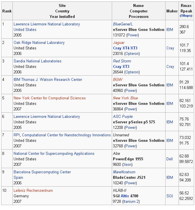
Since the Cray T3E, supercomputers have steadily improved their shared address space architectures. Many of the improvements in address space organization have been utilized by supercomputers. Since the T3E was released, Cray merged with SGI and acquired OctigaBay Systems Corporation | Since the Cray T3E, supercomputers have steadily improved their shared address space architectures. Many of the improvements in address space organization have been utilized by supercomputers. Since the T3E was released, Cray merged with SGI and acquired OctigaBay Systems Corporation. As a leader in the development of supercomputers, Cray, Inc. has released several more machines superior to the T3E. The most noticeable feature in newer supercomputers is the implementation of distributed shared memory (DSM). Below are 10 of the fastest supercomputers in recent time. | ||
[[Image:Table01.JPG]] | |||
Figure 4.1 - Top 10 Fastest Supercomputers | |||
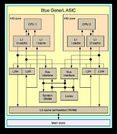
Ranked as the fastest supercomputer in the world and released after Cray's T3E, IBM's Blue Genie supercomputer is currently able to reach speeds of 367 TeraFlops. A node in the Blue Gene architecture consists of a single ASIC, shown in Figure 4.2, along with a read/write locking mechanism, scratch DRAM, and L1 and L2 data caches. The ASIC contains two 700 MHz PowerPC 440 embedded processors. Each of the processors has two floating point units, DRAM controller and the logic to support multiple message sharing system. Theoretically a peak performance of 5.6 GFLOPS can be acheived by the dual FPUs. To reduce overhead, peer node CPUs are not cache coherent. | |||
[[Image:Pic01.jpg]] | |||
Figure 4.2 - Blue Gene node ASIC | |||
Due to the nature of implementing the cores on ASIC chips, low power operation was maintained, allowing high area density and scalability of nodes. Each node operates in a range around 17 Watts. These properties allow up to 1024 nodes plus additional IO nodes in a standard 19" cabinet, within reasonable limits of electrical power supply and air cooling. | |||
A hybrid of bus and message passsing architectures are used in the Blue Gene as is necessary for high speed symmetric memory locations that allows scalability. Each node is part of a 3D toroidal bus network architecture, a bus network for collective communication, and a message passing global interrupt network. | |||
== References == | == References == | ||
[http://www.sun.com/servers/highend/sunfire12k/] Sunfire12k | |||
[http://www.cray.com/products/xt4/index.html] Cray XT4 | |||
[http://www-03.ibm.com/systems/uk/p/hardware/enterprise.html] IBM | |||
[http://www.cray.com/downloads/X1E_datasheet.pdf] Cray X1E | |||
[http://en.wikipedia.org/wiki/Vector_processor] Wikipedia: Vector Processor | |||
[http://en.wikipedia.org/wiki/Image:Blue_Gene_L_ASIC.png] Wikipedia: Blue Gene | |||
7. McCurdy , C. & Fischer, C. (2003). User-controllable coherence for high performance shared memory multiprocessors. Proceedings of the Ninth ACM SIGPLAN Symposium on Principles and Practice of Parallel Programming Archive, , 73-82. | |||
8. Culler, D. E., Singh, J. P., & Gupta, A. (1999). Introduction: Convergence of Parallel Architectures: Shared Address Space. In D. E. Penrose (Ed.), A Tutor's Guide: Helping Writers One to One (pp. 28-37). San Francisco, CA: Morgan Kaufmann. | |||
9. El-Rewini, Hesham. Abd-El-Barr, Mostafa. Advanced Computer Architecture and Parallel Processing (chapter 2 & 4), John Wiley & Sons, Inc. (US), 2005 | |||
Latest revision as of 03:27, 11 September 2007
Shared address space is an important class of the multiprocessors where all processors share a global memory. Communication between tasks running on different processors is performed through writing to and reading from the global memory. All interprocessor coordination and synchronization is also accomplished via the global memory. Hence, a shared memory computer system consists of a set of independent processors, a set of memory modules, and an interconnection network.
This article talks about the recent trends in shared address space and how the interconnection technology has changed in last 10 years. Later it highlights some of the existing SMPs and latest supercomputer.
Current high-performance multiprocessor platforms may be broken into two categories: distributed address-space and shared address-space. For programs running on a distributed address-space multiprocessor, data visible on one processing unit is not visible on the remaining processor units. In contrast, hardware mechanisms in high performance shared address-space environments ensure that all data is in principle visible to all processors. While a shared address-space can offer programmability advantages and better performance for fine-grained applications, the very mechanisms that create those advantages appear to prevent the machines from scaling to large numbers of processors.
To scale beyond the limits of traditional shared address space architectures, hybrids of shared and distributed architectures are becoming more prevalent. These architectures allow users to take advantage of two or more address spaces to gain the scalability of distributed architectures while retaining the benefits of the shared address-space architecture. Memory is split into global, which hardware keeps coherent, and strictly local, which is left incoherent. Application programmers are given a mechanism for specifying, at a very high level, data that would benefit from localization – being moved from global to local memory. This transparency in memory partitioning takes place through improved compiler allocation mechanisms than the traditional hardware devices. The following are benefits of localizing otherwise remote memory accesses.
1. Faster access to localized data.
2. Elimination of redundant protocol traffic.
3. Elimination of locking/contention for written shared data.
A trend in application design is the use of vector instructions. This allows programs to deliver more fine grain tasks which capitalize on the parallel processing nature of a shared address space architecture. Vector instructions, also known as SIMD (single intruction multiple data), have been optimized on a series of recent architectures including the cell processor in Toshiba/Sony's PlayStation 3 game console. The PS3 cell processor consists of one scalar and eight vector processors.
Evolution of Interconnect Technology
The effectiveness of the shared memory approach depends on the latency incurred on the memory access as well as the bandwidth of the data transfer that can be supported. The interconnection network in a shared-memory multiprocessor has evolved over a decade to provide better aggregate bandwidth when more processors are added without increasing cost too much. Shared memory systems can be designed using bus-based or switch-based interconnection networks. The simplest network for shared memory systems is the bus and moreover the bus/cache architecture alleviates the need for expensive multiported memories and interface circuitry as well as the need to adopt a message-passing paradigm when developing application software. The single shared bus system has been extended to multiple buses to connect multiple processors.
A multiple bus multiprocessor system uses several parallel buses to interconnect multiple processors and multiple memory modules. A number of connection schemes are possible in this case. Among the possibilities are the multiple bus with full bus–memory connection (MBFBMC), multiple bus with single bus memory connection (MBSBMC), multiple bus with partial bus–memory connection (MBPBMC), and multiple bus with class-based memory connection (MBCBMC). The multiple bus with full bus–memory connection has all memory modules connected to all buses. The multiple bus with single bus–memory connection has each memory module connected to a specific bus. The multiple bus with partial bus–memory connection has each memory module connected to a subset of buses. The multiple bus with class-based memory connection has memory modules grouped into classes whereby each class is connected to a specific subset of buses. A class is just an arbitrary collection of memory modules. Example of different multiple bus scheme for for the case of N = 6 processors, M = 4 memory modules, and B = 4 buses has been illustrated in the figure below.
Figure 2.1 (a) Multiple bus with full bus–memory connection (MBFBMC); (b) multiple bus with single bus-memory connection (MBSBMC); (c) multiple bus with partial bus–memory connection (MBPBMC); and (d) multiple bus with class-based memory connection (MBCBMC). [Source: Reference 8]
A typical bus-based design uses caches to solve the bus contention problem. Highspeed caches connected to each processor on one side and the bus on the other side mean that local copies of instructions and data can be supplied at the highest possible rate. If the local processor finds all of its instructions and data in the local cache, we say the hit rate is 100%. The miss rate of a cache is the fraction of the references that are not stored locally. The required data must be copied from the global memory, across the bus and into the cache. From there it is routed to the local processor. One of the goals of the cache is to maintain a low miss rate under high processor loads. A low miss rate means the processors do not have to use the bus as much. Miss rates are determined by a number of factors, ranging from the complexity and number of applications being run to the organization of the cache hardware that is implemented.
Current High End SMPs
Symmetric multiprocessors (SMPs) are available from a wide range of workstation vendors in various configurations. With the introduction of dual-core devices, SMP is found in most new desktop machines and in many laptop machines. The most popular entry-level SMP systems use the x86 instruction set architecture and are based on Intel’s Xeon, Pentium D, Core Duo, and Core 2 Duo based processors or AMD’s Athlon64 X2, Quad FX or Opteron 200 and 2000 series processors. Servers use those processors and other readily available non-x86 processor choices including the Sun Microsystems UltraSPARC, Fujitsu SPARC64, SGI MIPS, Intel Itanium, Hewlett Packard PA-RISC, Hewlett-Packard (formerly Compaq formerly Digital Equipment Corporation) DEC Alpha, IBM POWER and Apple Computer PowerPC (specifically G4 and G5 series, as well as earlier PowerPC 604 and 604e series) processors.
1. The Sun Fire 12K server is a high-end data center server with up to 52 UltraSPARC III Cu 1.2-GHz processors in a symmetric multiprocessing architecture. The Sun Fire E52K server scales up to 72 UltraSPARC IV+ processors.
2. The Cray XT4 system can scale from 562 to 30,614 AMD Dual Core 2.6-GHz giving a peak performance varying from 5.6TFLOPS to 318 TFLOPS.
3. The IBM System p5 595 server uses fifth-generation 64-bit IBM POWER5 technology in up to 64 core symmetric multi-processing (SMP) configurations with IBM Advanced POWER5+ (2.1/2.3GHz).
Evolution of Supercomputers
Since the Cray T3E, supercomputers have steadily improved their shared address space architectures. Many of the improvements in address space organization have been utilized by supercomputers. Since the T3E was released, Cray merged with SGI and acquired OctigaBay Systems Corporation. As a leader in the development of supercomputers, Cray, Inc. has released several more machines superior to the T3E. The most noticeable feature in newer supercomputers is the implementation of distributed shared memory (DSM). Below are 10 of the fastest supercomputers in recent time.
Figure 4.1 - Top 10 Fastest Supercomputers
Ranked as the fastest supercomputer in the world and released after Cray's T3E, IBM's Blue Genie supercomputer is currently able to reach speeds of 367 TeraFlops. A node in the Blue Gene architecture consists of a single ASIC, shown in Figure 4.2, along with a read/write locking mechanism, scratch DRAM, and L1 and L2 data caches. The ASIC contains two 700 MHz PowerPC 440 embedded processors. Each of the processors has two floating point units, DRAM controller and the logic to support multiple message sharing system. Theoretically a peak performance of 5.6 GFLOPS can be acheived by the dual FPUs. To reduce overhead, peer node CPUs are not cache coherent.
Figure 4.2 - Blue Gene node ASIC
Due to the nature of implementing the cores on ASIC chips, low power operation was maintained, allowing high area density and scalability of nodes. Each node operates in a range around 17 Watts. These properties allow up to 1024 nodes plus additional IO nodes in a standard 19" cabinet, within reasonable limits of electrical power supply and air cooling.
A hybrid of bus and message passsing architectures are used in the Blue Gene as is necessary for high speed symmetric memory locations that allows scalability. Each node is part of a 3D toroidal bus network architecture, a bus network for collective communication, and a message passing global interrupt network.
References
[1] Sunfire12k
[2] Cray XT4
[3] IBM
[4] Cray X1E
[5] Wikipedia: Vector Processor
[6] Wikipedia: Blue Gene
7. McCurdy , C. & Fischer, C. (2003). User-controllable coherence for high performance shared memory multiprocessors. Proceedings of the Ninth ACM SIGPLAN Symposium on Principles and Practice of Parallel Programming Archive, , 73-82.
8. Culler, D. E., Singh, J. P., & Gupta, A. (1999). Introduction: Convergence of Parallel Architectures: Shared Address Space. In D. E. Penrose (Ed.), A Tutor's Guide: Helping Writers One to One (pp. 28-37). San Francisco, CA: Morgan Kaufmann.
9. El-Rewini, Hesham. Abd-El-Barr, Mostafa. Advanced Computer Architecture and Parallel Processing (chapter 2 & 4), John Wiley & Sons, Inc. (US), 2005


