CSC/ECE 506 Spring 2013/1a sp: Difference between revisions
| Line 30: | Line 30: | ||
Some major implementations of MISD are in the fields of systolic arrays, pattern matching, flight control systems and fault tolerance systems. These MISD implementations are discussed below. | Some major implementations of MISD are in the fields of systolic arrays, pattern matching, flight control systems and fault tolerance systems. These MISD implementations are discussed below. | ||
=== | ===Systolic Array=== | ||
A systolic array is an arrangement of processors in an array where data flows synchronously across the array between neighbors, usually with different data flowing in different directions. Each Processor at each step takes in data from one or more neighbors, processes it and, in the next step, outputs results in the opposite direction. | A systolic array is an arrangement of processors in an array where data flows synchronously across the array between neighbors, usually with different data flowing in different directions. Each Processor at each step takes in data from one or more neighbors, processes it and, in the next step, outputs results in the opposite direction. | ||
| Line 36: | Line 36: | ||
The systolic array paradigm, data-stream-driven by data counters, is the counterpart of the [http://en.wikipedia.org/wiki/Von_Neumann_model von Neumann paradigm], instruction-stream-driven by a program counter. Because a systolic array usually sends and receives multiple data streams, and multiple data counters are needed to generate these data streams, it supports data parallelism. The name derives from analogy with the regular pumping of blood by the heart.<ref>http://en.wikipedia.org/wiki/Systolic_array</ref> | The systolic array paradigm, data-stream-driven by data counters, is the counterpart of the [http://en.wikipedia.org/wiki/Von_Neumann_model von Neumann paradigm], instruction-stream-driven by a program counter. Because a systolic array usually sends and receives multiple data streams, and multiple data counters are needed to generate these data streams, it supports data parallelism. The name derives from analogy with the regular pumping of blood by the heart.<ref>http://en.wikipedia.org/wiki/Systolic_array</ref> | ||
==== | ====Type of Systolic Arrays<ref>http://home.engineering.iastate.edu/~zambreno/classes/cpre583/documents/JohHur93A.pdf General Purpose Systolic Arrays </ref>==== | ||
===== | =====Special-purpose systolic array===== | ||
[[Image:systolic_1.png|thumb|right|250px|Figure 3: The algorithm for the sum of a scalar product, computed in systolic element [[http://expertiza.csc.ncsu.edu/wiki/index.php/CSC/ECE_506_Spring_2012/1c_dm#cite_note-4 5]]]] | [[Image:systolic_1.png|thumb|right|250px|Figure 3: The algorithm for the sum of a scalar product, computed in systolic element [[http://expertiza.csc.ncsu.edu/wiki/index.php/CSC/ECE_506_Spring_2012/1c_dm#cite_note-4 5]]]] | ||
[[Image:systolic_2.png|thumb|right|250px|Figure 7: The systolic product of two 3x3 matrices [[http://expertiza.csc.ncsu.edu/wiki/index.php/CSC/ECE_506_Spring_2012/1c_dm#cite_note-4 5]]]] | [[Image:systolic_2.png|thumb|right|250px|Figure 7: The systolic product of two 3x3 matrices [[http://expertiza.csc.ncsu.edu/wiki/index.php/CSC/ECE_506_Spring_2012/1c_dm#cite_note-4 5]]]] | ||
| Line 44: | Line 44: | ||
An array of hardwired systolic processing elements tailored for a specific application. Typically, many tens or hundreds of cells fit on a single chip. One of the major applications of special-purpose systolic array is in matrix operations. [http://expertiza.csc.ncsu.edu/wiki/index.php/File:Systolic_1.png Figure 3] illustrates the algorithm for the sum of a scalar product, computed in a single systolic element. Here, a’s and b’s are synchronously shifted through the processing element to be available for next element. These data synchronously exits the processing element unmodified for the next element. The sum of the products is then shifted out of the accumulator. | An array of hardwired systolic processing elements tailored for a specific application. Typically, many tens or hundreds of cells fit on a single chip. One of the major applications of special-purpose systolic array is in matrix operations. [http://expertiza.csc.ncsu.edu/wiki/index.php/File:Systolic_1.png Figure 3] illustrates the algorithm for the sum of a scalar product, computed in a single systolic element. Here, a’s and b’s are synchronously shifted through the processing element to be available for next element. These data synchronously exits the processing element unmodified for the next element. The sum of the products is then shifted out of the accumulator. | ||
===== | =====General-purpose systolic array===== | ||
It is an array of systolic processing elements, which gets adapted to a variety of applications via programming or reconfiguration. Array topologies can be either programmable or reconfigurable. Likewise, array cells are either programmable or reconfigurable. This is referred to as Systolic topologies. | It is an array of systolic processing elements, which gets adapted to a variety of applications via programming or reconfiguration. Array topologies can be either programmable or reconfigurable. Likewise, array cells are either programmable or reconfigurable. This is referred to as Systolic topologies. | ||
===== | ======Programmable Systolic Array====== | ||
It is an array of programmable systolic elements that operates either in SIMD or MIMD fashion. Either the arrays interconnect or each processing unit is programmable and a program controls dataflow through the elements. Programmable systolic arrays are programmable either at a high level or a low level. At either level, programmable arrays can be categorized as either SIMD or MIMD machines. | It is an array of programmable systolic elements that operates either in SIMD or MIMD fashion. Either the arrays interconnect or each processing unit is programmable and a program controls dataflow through the elements. Programmable systolic arrays are programmable either at a high level or a low level. At either level, programmable arrays can be categorized as either SIMD or MIMD machines. | ||
| Line 58: | Line 58: | ||
This architecture is defined as Multiple Instruction Multiple Data (MIMD) architecture in [http://home.engineering.iastate.edu/~zambreno/classes/cpre583/documents/JohHur93A.pdf 5]. The architecture has multiple instruction streams for the PEs and a single data stream passing through all the PEs. Thus, it can also be defined as Multiple Instruction Single Data (MISD) architecture. The architecture of Systolic array configuration are controversial as explained in the [http://expertiza.csc.ncsu.edu/wiki/index.php/CSC/ECE_506_Spring_2012/1c_dm#Architecture_of_systolic_arrays_as_against_MISD_architecture section 4.1.2.] | This architecture is defined as Multiple Instruction Multiple Data (MIMD) architecture in [http://home.engineering.iastate.edu/~zambreno/classes/cpre583/documents/JohHur93A.pdf 5]. The architecture has multiple instruction streams for the PEs and a single data stream passing through all the PEs. Thus, it can also be defined as Multiple Instruction Single Data (MISD) architecture. The architecture of Systolic array configuration are controversial as explained in the [http://expertiza.csc.ncsu.edu/wiki/index.php/CSC/ECE_506_Spring_2012/1c_dm#Architecture_of_systolic_arrays_as_against_MISD_architecture section 4.1.2.] | ||
===== | ======Reconfigurable Systolic Array====== | ||
[[Image:reconfig.jpg|thumb|right|250px|Figure 10: Block Diagram of the RSA Architecture [http://expertiza.csc.ncsu.edu/wiki/index.php/CSC/ECE_506_Spring_2012/1c_dm#cite_note-4 5]]] | [[Image:reconfig.jpg|thumb|right|250px|Figure 10: Block Diagram of the RSA Architecture [http://expertiza.csc.ncsu.edu/wiki/index.php/CSC/ECE_506_Spring_2012/1c_dm#cite_note-4 5]]] | ||
It is an array of systolic elements that can be programmed at the lowest level. Recent gate density advances in FPGA technology have produced a low-level, reconfigurable systolic array architecture that bridges the gap between special-purpose arrays and the more versatile, programmable general-purpose arrays. The FPGA architecture is unusual because a single hardware platform can be logically reconfigured as an exact duplicate of a special-purpose systolic array. | It is an array of systolic elements that can be programmed at the lowest level. Recent gate density advances in FPGA technology have produced a low-level, reconfigurable systolic array architecture that bridges the gap between special-purpose arrays and the more versatile, programmable general-purpose arrays. The FPGA architecture is unusual because a single hardware platform can be logically reconfigured as an exact duplicate of a special-purpose systolic array. | ||
| Line 64: | Line 64: | ||
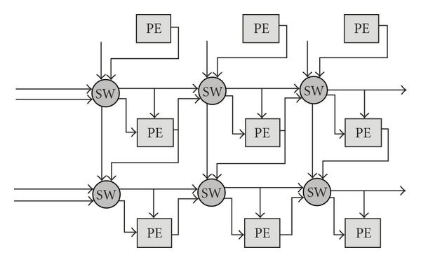
The RSA circuit design is based on systolic array architecture consisting of PEs interconnected via SWs as depicted in [http://expertiza.csc.ncsu.edu/wiki/index.php/File:Reconfig.jpg Figure 10]. The homogeneous characteristic of the Reconfigurable Systolic Array (RSA) architecture, where each reconfigurable processing element (PE) cell is connected to its nearest neighbors via configurable switch (SW) elements, enables array expansion for parallel processing and facilitates time sharing computation of high-throughput data by individual PEs. Both the PEs and SWs can be reconfigured dynamically with the former as an arithmetic processor and the latter as a flexible router linking the neighboring PE cells. The RSA shifts reconfiguration and input signals into the PEs and SWs on separate data bus which enables the circuit to continue its operation while the reconfiguration is in process. | The RSA circuit design is based on systolic array architecture consisting of PEs interconnected via SWs as depicted in [http://expertiza.csc.ncsu.edu/wiki/index.php/File:Reconfig.jpg Figure 10]. The homogeneous characteristic of the Reconfigurable Systolic Array (RSA) architecture, where each reconfigurable processing element (PE) cell is connected to its nearest neighbors via configurable switch (SW) elements, enables array expansion for parallel processing and facilitates time sharing computation of high-throughput data by individual PEs. Both the PEs and SWs can be reconfigured dynamically with the former as an arithmetic processor and the latter as a flexible router linking the neighboring PE cells. The RSA shifts reconfiguration and input signals into the PEs and SWs on separate data bus which enables the circuit to continue its operation while the reconfiguration is in process. | ||
==== | ====Architecture of systolic arrays as against MISD architecture==== | ||
[[Image:comp.png|thumb|right|250px|Figure 11.Comparison between Architecture of systolic arrays and MISD]] | [[Image:comp.png|thumb|right|250px|Figure 11.Comparison between Architecture of systolic arrays and MISD]] | ||
| Line 71: | Line 71: | ||
Many authors say that as the data read as input by one processing element is processed data output of the adjacent PE. The data stream cannot be considered as single because all the data paths do not carry the same data to all the PEs. [http://expertiza.csc.ncsu.edu/wiki/index.php/File:Comp.png Figure 11] shows the difference between the Data Stream for Systolic Arrays and the MISD architecture. Thus the systolic array should be considered as “Multiple Data” architecture and not Single Data architecture. | Many authors say that as the data read as input by one processing element is processed data output of the adjacent PE. The data stream cannot be considered as single because all the data paths do not carry the same data to all the PEs. [http://expertiza.csc.ncsu.edu/wiki/index.php/File:Comp.png Figure 11] shows the difference between the Data Stream for Systolic Arrays and the MISD architecture. Thus the systolic array should be considered as “Multiple Data” architecture and not Single Data architecture. | ||
=== | ===Fault Tolerant Systems<ref>http://en.wikipedia.org/wiki/Fault-tolerant_computer_system#Types_of_fault_tolerance</ref>=== | ||
The fault tolerant systems are designed to handle the possible failures in software, hardware or interfaces. The hardware faults include hard disk failures, input or output device failures, etc. and the software and interface faults include driver failures; operator errors, installing unexpected software etc. The hardware faults can be detected and identified by implementing redundant hardware and multiple backups. The software faults can be tolerable by removing the program errors by executing the software redundantly or by implementing small programs that take over the tasks that crash or generate errors. | The fault tolerant systems are designed to handle the possible failures in software, hardware or interfaces. The hardware faults include hard disk failures, input or output device failures, etc. and the software and interface faults include driver failures; operator errors, installing unexpected software etc. The hardware faults can be detected and identified by implementing redundant hardware and multiple backups. The software faults can be tolerable by removing the program errors by executing the software redundantly or by implementing small programs that take over the tasks that crash or generate errors. | ||
| Line 81: | Line 81: | ||
There are various examples of [http://expertiza.csc.ncsu.edu/wiki/index.php/CSC/ECE_506_Spring_2012/1c_dm#Multiple_Instructions.2C_Single_Data_stream_.28MISD.29 MISD architecture] being used as fault tolerant architecture. The major examples being flight control systems, nuclear power plants, satellite systems, super collider experiment systems, etc. Here, the flight control system is explained as an example of [http://expertiza.csc.ncsu.edu/wiki/index.php/CSC/ECE_506_Spring_2012/1c_dm#Multiple_Instructions.2C_Single_Data_stream_.28MISD.29 MISD architecture]. | There are various examples of [http://expertiza.csc.ncsu.edu/wiki/index.php/CSC/ECE_506_Spring_2012/1c_dm#Multiple_Instructions.2C_Single_Data_stream_.28MISD.29 MISD architecture] being used as fault tolerant architecture. The major examples being flight control systems, nuclear power plants, satellite systems, super collider experiment systems, etc. Here, the flight control system is explained as an example of [http://expertiza.csc.ncsu.edu/wiki/index.php/CSC/ECE_506_Spring_2012/1c_dm#Multiple_Instructions.2C_Single_Data_stream_.28MISD.29 MISD architecture]. | ||
==== | ====The Flight Control System – MISD Example for fault tolerance==== | ||
A [http://en.wikipedia.org/wiki/Fly-by-wire Fly-By-Wire] system is used to replace the manual flight control by an electronic control interface. The movements of the flight control in the cockpit are converted to electronic signals and are transmitted to the actuators by wires. The control computers use the feedback from the sensors to compute and control the movement of the actuators to provide the expected response. These computers also perform the task to stabilize the aircraft and perform other tasks without the knowledge of the pilot. Flight control systems must meet extremely high levels of accuracy and functional integrity. | A [http://en.wikipedia.org/wiki/Fly-by-wire Fly-By-Wire] system is used to replace the manual flight control by an electronic control interface. The movements of the flight control in the cockpit are converted to electronic signals and are transmitted to the actuators by wires. The control computers use the feedback from the sensors to compute and control the movement of the actuators to provide the expected response. These computers also perform the task to stabilize the aircraft and perform other tasks without the knowledge of the pilot. Flight control systems must meet extremely high levels of accuracy and functional integrity. | ||
| Line 97: | Line 97: | ||
The above mentioned system clearly has individual Instruction Streams as the architecture of each processor is different, thus different instruction sets and different instruction streams. These processors have frame synchronized input data which means they have same set of data to work upon which is fed from a single data stream. Thus the flight control system can be classified under MISD architecture. | The above mentioned system clearly has individual Instruction Streams as the architecture of each processor is different, thus different instruction sets and different instruction streams. These processors have frame synchronized input data which means they have same set of data to work upon which is fed from a single data stream. Thus the flight control system can be classified under MISD architecture. | ||
=== | ===Edge Detection of Images on TMS320C80 Multiprocessor System=== | ||
The image pre-processing system of this Multiprocessor [9] , the pre-image processing time needed to be made shorter. To achieve the aim of reducing the pre-processing time, different types of image processing architectures for ‘C80 were presented. For example MIMD architecture is used for image histogram equalization; SIMD architecture for median filtering; MISD architecture for directional edge detection. | The image pre-processing system of this Multiprocessor [9] , the pre-image processing time needed to be made shorter. To achieve the aim of reducing the pre-processing time, different types of image processing architectures for ‘C80 were presented. For example MIMD architecture is used for image histogram equalization; SIMD architecture for median filtering; MISD architecture for directional edge detection. | ||
| Line 112: | Line 112: | ||
5 PP3 Logic Filtering | 5 PP3 Logic Filtering | ||
Table 1: Pipeline structure for image edge detection [9] | Table 1: Pipeline structure for image edge detection [9] | ||
=='''References'''== | =='''References'''== | ||
Revision as of 22:47, 4 February 2013
Multiple Instruction Single Data (MISD) Architecture
Multiple Instruction Single Data, or MISD, architecture is one of the four general categories of multi-processor or multi-core architectures described by Flynn's Taxonomy.
MISD Architectures within the Context of Flynn’s Taxonomy<ref>http://en.wikipedia.org/wiki/Flynn's_taxonomy</ref><ref>http://www.phy.ornl.gov/csep/ca/node11.html</ref>
Flynn's Taxonomy categorizes parallel computing architectures based on the number of information streams that flowed into the processor. According to Flynn's Taxonomy, there are two kinds of logical streams of information that flows into a parallel computer, the Instruction Stream and the Data stream. Note that for the purposes of classification using Flynn’s Taxonomy, it does not matter whether or not the streams are physically independent of each other on the hardware, only that the streams can be logically treated as independent. Based on how many of each type of stream flows into the parallel computer (single vs. multiple), Flynn's Taxonomy divides parallel architectures into four categories. They are Single Instruction Single Data (SISD), Single Instruction Multiple Data (SIMD), Multiple Instruction Single Data (MISD), and Multiple Instruction Multiple Data (MIMD).
The four classifications defined by Flynn are based upon the number of concurrent instruction (or control) and data streams available in the architecture are<ref>https://computing.llnl.gov/tutorials/parallel_comp/#Flynn</ref>

Overview of the MISD Architecture
In order to be categorized as MISD architecture, there must be at least two Instruction streams and there can only be one Data stream as shown on Figure 2. As per the description according to Flynn’s Taxonomy, each processing elements should receive the same data and execute different instructions on the same data simultaneously.

There are very few implementations of the classical MISD architecture as described by Flynn’s Taxonomy, none of which are commercial, general purpose parallel computers. Instead, MISD architectures are mainly used to create custom hardware in order to solve specific problems. The majority of the implementations have been created are in academia. Over the years, several architectures have been described as MISD even though the architectures do not completely follow the description in Flynn’s Taxonomy. One common example is the Pipeline architecture where the data is passed from processing element to processing element and each processing element executes a different instruction. It is often argued that this is not a true MISD architecture as the data changes as it moves through the pipeline. Similarly, other architectures or applications exist which may be called MISD by some while others disagree. The following section looks at some of those implementations.
Pipeline architectures belong to this type, though a purist might say that the data is different after processing by each stage in the pipeline. Fault-tolerant computers executing the same instructions redundantly in order to detect and mask errors, in a manner known as task replication, may be considered to belong to this type. Not many instances of this architecture exist, as MIMD and SIMD are often more appropriate for common data parallel techniques. Specifically, they allow better scaling and use of computational resources than MISD does.
However, one prominent example of MISD in computing is the Space Shuttle flight control computers. Another example of this machine is the systolic array, such as the CMU iWrap [BORKAR et al., 1990]. All the elements in this array are controlled by a global clock. On each cycle, an element will read a piece of data from one of its neighbors, perform a simple operation (e.g. add the incoming element to a stored value), and prepare a value to be written to a neighbor on the next step.
Implementations of MISD architecture
Some major implementations of MISD are in the fields of systolic arrays, pattern matching, flight control systems and fault tolerance systems. These MISD implementations are discussed below.
Systolic Array
A systolic array is an arrangement of processors in an array where data flows synchronously across the array between neighbors, usually with different data flowing in different directions. Each Processor at each step takes in data from one or more neighbors, processes it and, in the next step, outputs results in the opposite direction.
The systolic array paradigm, data-stream-driven by data counters, is the counterpart of the von Neumann paradigm, instruction-stream-driven by a program counter. Because a systolic array usually sends and receives multiple data streams, and multiple data counters are needed to generate these data streams, it supports data parallelism. The name derives from analogy with the regular pumping of blood by the heart.<ref>http://en.wikipedia.org/wiki/Systolic_array</ref>
Type of Systolic Arrays<ref>http://home.engineering.iastate.edu/~zambreno/classes/cpre583/documents/JohHur93A.pdf General Purpose Systolic Arrays </ref>
Special-purpose systolic array
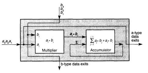
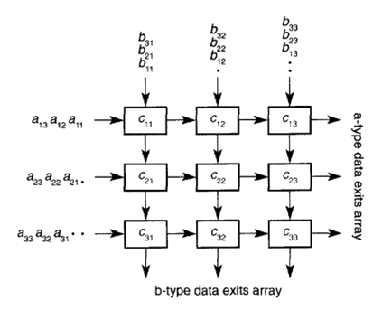
An array of hardwired systolic processing elements tailored for a specific application. Typically, many tens or hundreds of cells fit on a single chip. One of the major applications of special-purpose systolic array is in matrix operations. Figure 3 illustrates the algorithm for the sum of a scalar product, computed in a single systolic element. Here, a’s and b’s are synchronously shifted through the processing element to be available for next element. These data synchronously exits the processing element unmodified for the next element. The sum of the products is then shifted out of the accumulator.
General-purpose systolic array
It is an array of systolic processing elements, which gets adapted to a variety of applications via programming or reconfiguration. Array topologies can be either programmable or reconfigurable. Likewise, array cells are either programmable or reconfigurable. This is referred to as Systolic topologies.
Programmable Systolic Array
It is an array of programmable systolic elements that operates either in SIMD or MIMD fashion. Either the arrays interconnect or each processing unit is programmable and a program controls dataflow through the elements. Programmable systolic arrays are programmable either at a high level or a low level. At either level, programmable arrays can be categorized as either SIMD or MIMD machines.
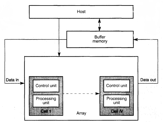
For the latter approach, the workstation downloads a program to each MIMD (Figure 7) systolic cell. Each cell may be loaded with a different program, or all the cells in the array may be loaded with the same program. Each cell's architecture is somewhat similar to the conventional von Neumann architecture: It contains a control unit, an ALU, and local memory. MIMD systolic cells have more local memory than their SIMD counterparts to support the von Neumann-style organization.
This architecture is defined as Multiple Instruction Multiple Data (MIMD) architecture in 5. The architecture has multiple instruction streams for the PEs and a single data stream passing through all the PEs. Thus, it can also be defined as Multiple Instruction Single Data (MISD) architecture. The architecture of Systolic array configuration are controversial as explained in the section 4.1.2.
Reconfigurable Systolic Array
It is an array of systolic elements that can be programmed at the lowest level. Recent gate density advances in FPGA technology have produced a low-level, reconfigurable systolic array architecture that bridges the gap between special-purpose arrays and the more versatile, programmable general-purpose arrays. The FPGA architecture is unusual because a single hardware platform can be logically reconfigured as an exact duplicate of a special-purpose systolic array.
The RSA circuit design is based on systolic array architecture consisting of PEs interconnected via SWs as depicted in Figure 10. The homogeneous characteristic of the Reconfigurable Systolic Array (RSA) architecture, where each reconfigurable processing element (PE) cell is connected to its nearest neighbors via configurable switch (SW) elements, enables array expansion for parallel processing and facilitates time sharing computation of high-throughput data by individual PEs. Both the PEs and SWs can be reconfigured dynamically with the former as an arithmetic processor and the latter as a flexible router linking the neighboring PE cells. The RSA shifts reconfiguration and input signals into the PEs and SWs on separate data bus which enables the circuit to continue its operation while the reconfiguration is in process.
Architecture of systolic arrays as against MISD architecture
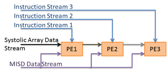
As from the above mentioned configurations of the Systolic Arrays, it is seen that generally the configurations have multiple processing elements executing different instructions from dedicated instruction streams for each processing element. There is a single data stream that connects the adjacent PEs. Thus, systolic array can be defined as an MISD architecture.
Many authors say that as the data read as input by one processing element is processed data output of the adjacent PE. The data stream cannot be considered as single because all the data paths do not carry the same data to all the PEs. Figure 11 shows the difference between the Data Stream for Systolic Arrays and the MISD architecture. Thus the systolic array should be considered as “Multiple Data” architecture and not Single Data architecture.
Fault Tolerant Systems<ref>http://en.wikipedia.org/wiki/Fault-tolerant_computer_system#Types_of_fault_tolerance</ref>
The fault tolerant systems are designed to handle the possible failures in software, hardware or interfaces. The hardware faults include hard disk failures, input or output device failures, etc. and the software and interface faults include driver failures; operator errors, installing unexpected software etc. The hardware faults can be detected and identified by implementing redundant hardware and multiple backups. The software faults can be tolerable by removing the program errors by executing the software redundantly or by implementing small programs that take over the tasks that crash or generate errors.
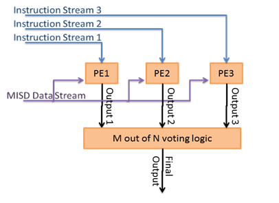
In computer systems, the SIMD, MISD and MIMD architectures facilitate the implementation of the fault tolerance systems by multiple instruction streams or multiple data streams or both. Fault tolerance on computations can be implemented by multiple processors (likely with different architectures) executing the algorithms on the same set of data. The output of each processor is compared with that of the others and M out of N majority voting method is used to determine the faulty processor. Thus MISD architecture is utilized to get the fault tolerance on critical computations.
There are various examples of MISD architecture being used as fault tolerant architecture. The major examples being flight control systems, nuclear power plants, satellite systems, super collider experiment systems, etc. Here, the flight control system is explained as an example of MISD architecture.
The Flight Control System – MISD Example for fault tolerance
A Fly-By-Wire system is used to replace the manual flight control by an electronic control interface. The movements of the flight control in the cockpit are converted to electronic signals and are transmitted to the actuators by wires. The control computers use the feedback from the sensors to compute and control the movement of the actuators to provide the expected response. These computers also perform the task to stabilize the aircraft and perform other tasks without the knowledge of the pilot. Flight control systems must meet extremely high levels of accuracy and functional integrity.
There are redundant flight control computers present in the flight control system. If one of the flight-control computers crashes, gets damaged or is affected by electromagnetic pulses, the other computer can overrule the faulty one and hence the flight of the aircraft is unharmed.
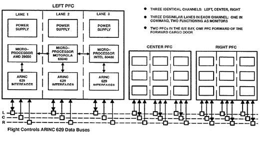
The number of redundant flight control computers is generally more than two, so that any computer whose results disagree with the others is ruled out to be faulty and is either ignored or rebooted.
Multiple Processors Implementation in Boeing 777<ref>http://www.citemaster.net/getdoc/8767/R8.pdf Y.C. (Bob) Yeh, Boeing Commercial Airplane Group, "Triple-Triple Redundant 777 Primary Flight Computer" </ref>
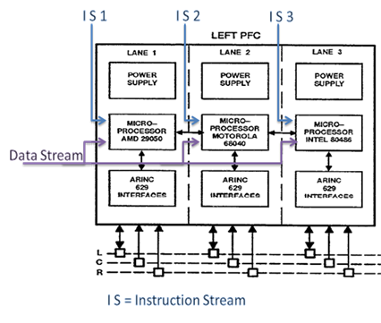
In modern computers, the redundant flight control computations are carried out by multiprocessor systems. The triple redundant 777 primary flight computer, has the architecture as shown in Figure 13.
The system has three primary flight control computers, each of them having three lanes with different processors. The flight control program is compiled for each of the processors which get the input data from the same data bus but drive the output on their individual control bus. Thus each processor executes different instructions but they process the same data. Thus, it is the best suited example of Multiple Instruction Single Data (MISD) architecture.
The three processors selected for the flight control system of Boeing 777 were Intel 80486, Motorola 68040 and AMD 29050. The dissimilar processors lead to dissimilar interface hardware circuits and compilers. Each lane of the flight control computer is data synchronized with the other lanes so that all of the lanes read the same frame of data from the flight sensors. As the outputs of each lane can be different, the median value of the outputs is used to select the output of the lane to be considered. The lane which has the median value select hardware selected is said to be in “command mode” whereas the other lanes are said to be in “monitoring mode”. It receives the data from the other Primary Flight Computer (PFC) lanes and performs a median select of the outputs. This provides a fault blocking mechanism before the fault detection and identification by the cross-lane monitoring system. Thus, the MISD based multi computer architecture is capable of detecting generic errors in compilers or in complex hardware devices providing assurance beyond reasonable doubt of the dependability of the Fly-By-Wire system.
The above mentioned system clearly has individual Instruction Streams as the architecture of each processor is different, thus different instruction sets and different instruction streams. These processors have frame synchronized input data which means they have same set of data to work upon which is fed from a single data stream. Thus the flight control system can be classified under MISD architecture.
Edge Detection of Images on TMS320C80 Multiprocessor System
The image pre-processing system of this Multiprocessor [9] , the pre-image processing time needed to be made shorter. To achieve the aim of reducing the pre-processing time, different types of image processing architectures for ‘C80 were presented. For example MIMD architecture is used for image histogram equalization; SIMD architecture for median filtering; MISD architecture for directional edge detection.
The MISD architecture can be explained as follows. Here, each processor performs different operations on the same data set. It is mentioned at many places that MISD architecture was defined only for the sake of completeness of classification due to difficulty in practice to find a computer based on MISD architecture [10]. But in case of Image Processing, this assumption need not be true as here making many different operations on same image is rare and hence MISD architecture is a best fit for such cases. As an example of implementation of image processing operations for the MISD architecture the edge detection operation will be considered. The edges should be detected in four different directions (north, south, west and east) by the medium of four different filter masks. Each of the parallel processors of the TMS320C80 calculates one of the directional edges. Finally one obtains four images with detected edges, each in different direction.
The image processing in computer is very often a multistage process composed of many stages. For example, an algorithm detecting contours of the objects in an image. The algorithm for achieving the before mentioned is composed of four basic image processing operation. The image acquired from the camera in the first step undergoes low-pass filtering, during which it is smoothed and noise is also eliminated. In the next step image is thresholding is performed and each pixel gets black or white depending on that if its grey level is below or above threshold value. The resulting image is a binary image from which edges are detected by the usage of the Laplace filter. In the last step the image with detected contours undergoes logic filtering in the purpose of elimination of single black pixels placed on the white background. For implementing the above processes parallel, a five-stage pipeline was used. The first stage of this pipeline constitutes the master processor which accounts for control of the image acquisition process. Further pipe line stages were implemented for 4 parallel processors as mentioned in table 1.
Stage Processor Operation 1 MP Image acquisition 2 PP0 Low-pass Filtering 3 PP1 Thresholding 4 PP2 Laplace Filtering 5 PP3 Logic Filtering Table 1: Pipeline structure for image edge detection [9]
References
<references/>
Glossary
- CMU: Carnegie Mellon University
- CU: Control Unit
- DS: Data Stream
- Fly-By-Wire: System that replaces the conventional manual flight controls of an aircraft with an electronic interface
- FPGA: Field Programmable Gate Array
- Heterogeneous Systems: A multiprocessor system with different kind of processors
- Homogeneous System: A multiprocessor system with same kind of processors
- ILP: Instruction Level Parallelism
- IS: Instruction Stream
- MIMD: Multiple Instruction Multiple Data
- MISD: Multiple Instruction Single Data
- PE: Processing Element
- PFC: Primary Flight Computer
- SAPO: Short for Samočinný počítač
- SIMD: Single Instruction Multiple Data
- SISD: Single Instruction Single Data
- VLSI: Very Large Scale Integration