CSC/ECE 506 Spring 2012/6b am
With the present day processor speeds increasing at a much faster rate than memory speeds<ref>http://www.cesr.ncsu.edu/solihin/Main.html</ref>, there arises a need that the data transactions between the processor and the memory system be managed such that the slow memory speeds do not affect the performance of the processor system. While the read operations require that the processor wait for the read to complete before resuming execution, the write operations do not have this requirement. This is where a write buffer (WB) comes into the picture, assisting the processor in writes, so that the processor can continue its operation while the write buffer takes complete responsibility of executing the write. Use of a write buffer in this manner also frees up the cache to service read requests while the write is taking place. For a processor that operates at a speed much higher than the memory speed, this hardware scheme prevents performance bottlenecks caused by long-latency writes.<ref>http://en.wikipedia.org/wiki/Write_buffer</ref>
Introduction
Write Buffers in Uni-processors
Figure 1 shows the cache-based single processor system with a write buffer. A write to be performed is pushed into the buffer implemented as a FIFO (First In - First Out) queue, which essentially ensures that the writes are performed in the order that they were called. In a uni-processor model, with the requirement and possibility of extracting Instruction Level Parallelism (ILP), the writes may also be called out-of-order, provided there are some hardware/software protocols implemented to check the writes for any dependences that may exist in the instruction stream.
A generic approach towards read-write accesses can be described as follows [3][4]:
- If a write is followed by a read request to the same memory location while the write is still in the buffer, the buffered value is returned
- If a write is followed by a write request to the same memory location while the write is still in the buffer, the earlier write is overridden and is updated with the new write value
This follows that the write buffers not only save memory access overhead on the first write to a location, but also on the closely-spaced successive read-after-write and write-after-write sequences.
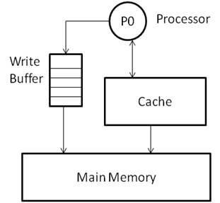
Interested reader may read about the store buffer and its implementation in ARM Cortex-R series processors.<ref>http://infocenter.arm.com/help/index.jsp?topic=/com.arm.doc.ddi0363e/Chdcahcf.html</ref><ref>http://infocenter.arm.com/help/index.jsp?topic=/com.arm.doc.ddi0246a/Cjafdjgj.html</ref>
Write Buffer Issues in Multiprocessors
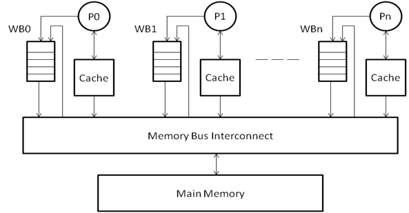
In a multiprocessor system, the same design can be extended, as shown in the Figure 2. In a generic design, each processor will have its own private cache and a write buffer corresponding to the cache. The caches are connected by the means of an interconnect with each other as well as with the main memory. As can be seen in the Figure 2, each processor makes a write by pushing it into its write buffer, and the write buffer completes the task of performing the write to the main memory or the cache. Consistency is maintained between ordering of memory accesses at individual processors in the same way as explained in the section above.
The Coherence Problem
However, with multiple processors working on the same task, it is essential that the memory ordering be consistent not only at individual processor level, but also with respect to all other processors in the system as well. Consider the case where a write (STORE A) has been issued by processor P1 into the WB1, and the write is waiting to be executed. Since the write has not yet been performed to the cache or the main memory, the other processors do not have any knowledge about the changes made to address A. As a result, a read operation by another processor from address A will take the value from either its own cache, write buffer, or the main memory (depending on whether it hits or misses in the cache).
This is a classic problem in all multi-processor systems, termed as Cache Coherence problem. It is the job of the designer to employ protocols that will take care of the sequential ordering of the instructions, and ensure that the writes made to any one of the caches are propagated and updated in all of the processor caches. With the addition of a write-buffer, we add another level to this problem, as we now have to ensure that pending write requests in a processor's buffer do not go unnoticed by other processors.
The sequential ordering model used in the system holds a strong bearing on the write buffer management policy, as is explained in a later section. We will now take a look at the definitions of different cache coherence policies and then move on to study various hardware implementations of the write buffer and the policies employed.
Coherence Models
"A memory scheme is coherent if the value returned on a LOAD instruction is always the value given by the latest STORE instruction with the same address."<ref>http://mprc.pku.cn/mentors/training/ISCAreading/1986/p434-dubois/p434-dubois.pdf</ref>
The two conventional models followed to attain this objective are the snoopy-bus protocol and the directory-based coherence protocol<ref>http://www.csl.cornell.edu/~heinrich/dissertation/ChapterTwo.pdf</ref>. The directory-based protocol is used for distributed memory systems, in which every processor keeps track of what data is being stored using a directory entry. In the snoopy-bus protocol, every processor monitors the reads and writes that are being serviced by the memory bus. The read and write requests can be broadcast on the bus for all the processors to respond based on whether or not they are in possession of that data in their cache.
With the addition of write buffers in the system, it is now essential that a processor be aware of the memory transactions occurring not only at the caches of other processors, but also in their write buffers. The snoopy bus protocol can maintain coherence between multiple write buffers by communicating using one of the two protocols explained below.
Write-Update
In this approach, a write request by a processor is first pushed onto its local write buffer, and then is broadcast on the bus for all other processors to see. Each processor updates its local cache and buffer with the new value of the data. This saves bus bandwidth in terms of writes, as there is only one broadcast that needs to be made in order for all the caches to be up to date with the newest value of the data. This is disadvantageous, however, when a snooped write transaction is present in a processor's cache - it needs to be updated right away, stalling other read operations that may be happening on that cache.
Write-Invalidate
This approach is common when dealing with systems where a data block is being written by one processor, but is being read by multiple processors. Whenever a write is made to shared data, it is pushed onto the local write buffer, and an invalidate signal is sent to all the caches and buffers, asking for that data block to be made invalid, as the value is not updated to the latest one. This approach alleviates us of the problem presented by the update protocol, as a snooped cache block is invalidated right away and does not keep any read waiting on the cache. However, this may cause additional traffic on the bus as a result, and a separate bus for invalidation requests may be included in the design.
Write–update strategy is liable to keep and update unnecessary data in the cache - the least recently used (LRU) algorithm may evict the useful data from the cache and keep the redundant updated data. Most present day processors employ write-invalidate policy because of its ease of implementation<ref>http://www.csl.cornell.edu/~heinrich/dissertation/ChapterTwo.pdf</ref>. In this article, for write-propagation of all hardware and software based designs we follow the write-invalidate strategy.
Coherence in Write Buffers
Software-Based Coherence
The software technique relies on the compiler to ensure that no dependencies exist between the STORE/LOAD accesses carried out at different processors on the shared memory. The compiler, based on indications from the programmer will make sure that there are no incoherent accesses to shared memory. There is a possibility of having a shared READ/WRITE buffer between all processors to access the main memory.
Hardware-Based Coherence
In hardware-based protocols accesses to the shared memory are communicated using hardware invalidate signals that are broadcasted to all the processor memories. Hardware support may also be required for a LOAD to be broadcasted to all the caches, so that a read can be performed directly from a remote memory. There are two approaches to maintaining coherence in write buffers and caches for multiprocessor system-
Unique Buffer per Processor<ref>http://mprc.pku.cn/mentors/training/ISCAreading/1986/p434-dubois/p434-dubois.pdf</ref>
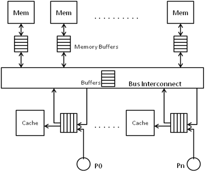
In this configuration, every processor has its own unique buffer that holds the loads and stores of the local processor as well as invalidates and loads of remote processors wanting access to the shared data. A store request in local cache will ensue invalidating of that data block in all other caches and main memory. A STORE is said to have been performed when
- the request is serviced in the buffer and the cache is updated on a local hit and
- the request is issued to the buffer and an invalidate request has been sent to all other processor on the shared data.
This can be achieved in two ways depending on the topology of the connection between the caches -
- For a bus-based MP system, the LOADs that miss in the local cache and the STOREs that need invalidation in other caches are broadcast over the bus to all processor caches and memory. The STORE request is then considered performed with respect to all processors when the invalidation signals have been sent out to the private buffers of all the caches.
- For non-bus MP systems, the caches are connected in point-to-point mesh-based or interconnect ring-based topology. When a store is encountered in one of the processors, the shared data is first locked in the shared memory to ensure atomic access, and then the invalidate signal is propagated along the point-to-point interconnect in a decided order. The STORE to shared memory is performed only when the invalidation has been propagated to all the processor caches and buffers. If any processor issues a LOAD on the same address as that is being STOREd, then the LOAD request has to be rejected or buffered to be serviced at a later time, to maintain atomic access to the shared data block.
Separate Buffers for Local and Remote Accesses<ref>http://mprc.pku.cn/mentors/training/ISCAreading/1986/p434-dubois/p434-dubois.pdf</ref>
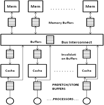
Another approach to maintaining coherence is for every processor to have separate buffers for local data requests and remote data requests. As seen in the figure, every processor has a Local-buffer which queues the local LOADs and STOREs, and a Remote-buffer (also termed Invalidate buffer) that stores the invalidation requests and LOADs coming in from different processors. In bus-based processor system, this approach makes it difficult to maintain write atomicity, as different invalidate buffers may hold different number of invalidation requests, putting uncertainty on the time to invalidate the concerned data block in the cache. In non-bus based systems, however, this approach is successful in maintaining strong coherence, provided the invalidate signal makes sure that the data is invalidated at a cache before moving on to the next processor (rather than just pushing the invalidate request in the buffers and moving on).
Universal read/write Buffer<ref>http://ieeexplore.ieee.org/xpl/freeabs_all.jsp?arnumber=342629&tag=1</ref>
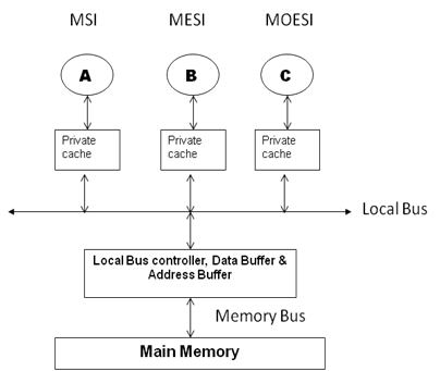
In this approach, a shared bus controller resides in between the local bus and memory bus, where local bus is connected to all private caches of the processors (illustrated in Figure 5). This technique supports multiple processors with same or different coherence protocols like; MSI, MESI and MOESI write invalidate strategy. Shared bus controller consists of the local bus controller, the data buffer and the address buffer. Each private cache provides two bit tri-state signals to the local bus – INTERVENE and SHARE.
- INTERVENE is asserted when any cache wants to provide a valid data to other caches.
- Cache controller asserts the SHARE when there is an address match with any of its own tag address.
Data Buffer
The data buffer consists of three FIFOs
- The non_block write-FIFO receives non cacheable memory access data from CPU. These requests do not require any cache eviction or line-fill cycles.
- The write-back FIFO is used for eviction cycles. If there is a cache miss and eviction is required, cache miss data will be read (line-fill cycle) from memory to the cache just after the evicted data moved to the FIFO. This FIFO will be written back to memory later on. So, CPU will get the new data but eviction process time will be hidden from the CPU.
- The read-FIFO is used for storing data from non_block write FIFO, Write-back FIFO or memory. Data is temporarily stored in this FIFO until local bus is cleared and ready for new data.
Address Buffer
The address buffer also consists of three FIFOs
- Non_block write FIFO - stores address of non-blocking accesses. The depth of this FIFO should be the same as the corresponding Data Buffer FIFO.
- Write-back FIFO - stores starting address of eviction cycle and holds the address until memory bus is free.
- Line-fill FIFO- stores the starting address of line-fill cycle.
Snoop logic is started whenever there is read access to main memory. Snoop logic compares the read request address with both write-back FIFO and line-fill FIFO. If there is a match, the HIT flag is set and CPU gets the data immediately through the internal bypass path. By doing so, stale data will not be read and the CPU doesn’t have to waste memory latency time.
For non_block write cycle, snoop logic block compares the new requested address and Byte Enable bits with the previously stored non_block write FIFO. If there is an address match but no Byte-Enable overlapped, BGO signal will be asserted and pointer of the non_block write FIFO will not move forward to prevent the FIFO from filling up quickly.
In this approach, the read access has priority over the write access, so whenever the memory bus is available, read address will get direct possession of the memory bus.
Local Bus Controller
Controller monitors the local bus for status bits (M, O, E, S, I), INTERVENE# and SHARE# bits and determines that a transaction needs to access main memory or private cache. For main memory access, controller informs the buffer with the signal of WB (Write Back), LF (Line Fill) or O3 (owned) status bit.
Algorithm to generate controller signals-
For the MSI and MOSI protocols:
- If there is a read miss on the local bus -INTERVENE is asserted.
- If there is a write miss with M status on the local bus, write back cycle will be performed -WB is asserted.
- If there is a read miss or write miss from any of the protocol LF cycle will be performed -LF is asserted.
For the MOESI protocol:
- If there is a read miss on the local bus -INTERVENE is asserted.
The above outputs can be written in Boolean equations as shown in the example<ref>http://ieeexplore.ieee.org/stamp/stamp.jsp?arnumber=00342629</ref> below:
     WB = RD * MOESI * INTV + WR * [STATUS=M]
     LF =  INTV
     03 = RD * MOESI * INTV
     MOESI means the cycle is initiated by MOESI protocol.
     INTV means INTERVENE signal which is asserted when any of cache provides a valid data to other cache.
Algorithms
The algorithm followed by each of the processors in a multiprocessor system is given below. The Processors may be following different protocols i.e. MSI/MESI/MOESI, but the algorithms below will ensure that the memory accesses are carried out coherently.
S state is common for all three protocols but this system takes the advantage of MESI and MOESI protocol by reducing memory bus transaction. In shared state(S), multiple caches have the same updated data but memory may or may not have a copy. This change requires the following protocol translation.
The algorithms for the MOESI protocol are as follows:
- If read hit initiated by other cache
- • M state provides data to other cache
- • Changes its state from M to O
- If same data is hit again
- • Cache with O state is responsible of providing data to the requesting cache.
- If read hit initiated by other cache
- If there is a write cache misses and INTERVENE is not activated
- • Generate a line-fill cycle
- If there is a write cache misses and INTERVENE is not activated
The algorithms for the MSI and MESI protocols are as follows. (These protocols have no O state) Algorithm for MSI protocol, M state provides data to the other caches & main memory and also changes the state from M to S. This transaction requires main memory access, but local bus translation logic plays a big role to reduce the bus access and improve performance.
- • Local Bus controller changes the status of MOESI to O instead of S
- • M of MSI or MESI changes to S and no update will occur on main memory.
- So, if same data is requested by other cache
- • O of MOESI will provide the data instead of main memory.
- If write cycle initiated
- If MOESI cache has a valid line with M or O
- MOESI cache will send out the data line on to local bus and change the state to I.
- (Because the line will be written and outdated by other cache.)
- If MOESI cache has a valid line with M or O
- If the status is E or S
- • No cache will involve of data transfer.
- • Main memory will provide the data.
Maintaining Sequential Consistency
When operating as a part of a multiprocessor, it is not enough to check dependencies between the writes only at the local level. As data is shared and the course of events in different processors may affect the outcomes of each other, it has to be ensured that the sequence of writes and the data dependencies is preserved between the multiprocessor. “A system is said to be sequentially consistent if the result of any execution is the same as if the operations of all the processors were executed in some sequential order, and the operation of each individual processor appear in this sequence in the order specified by its program.”<ref>http://www.cs.jhu.edu/~gyn/publications/memorymodels/node6.html</ref> There are different approaches to this requirement, based on the expected outcome of the program. The condition of sequential consistency and logical ordering may be relaxed as per the requirement of the program we are looking to parallelize.
Strong Ordering
The requirements for strong ordering are as follows:
1) All memory operations appear to execute one at a time.
2) All memory operations from a single CPU appear to execute in-order.
3) All memory operations from different processors are “cleanly” interleaved with each other (serialization)
Total Store Ordering
Requirements are as follows:
1) Relaxed Consistency where store must complete in-order but stores need not complete before a read to a given location takes place
2) Allows reads to bypass pending writes where writes MUST exit the store buffer in FIFO order.
Partial Store Ordering
Requirement is as follows:
Even more relaxed consistency where stores to any given memory location complete in-order but stores to different locations may complete out of order and stores need not complete before a read to a given location takes place.
Weak Ordering
Requirement is as follows:
Really relaxed consistency where anything goes, except at barrier synchronization points, global memory state must be completely settled at each synchronization and memory state may correspond to any ordering of reads and writes between synchronization points.
Example
Examples for Sequential Consistency: In the following program, consider variables “a”, “b”, “flag1” and “flag2” are initialized with 0 and both processors (CPU1 and CPU 2) are sharing all the variables
   a = b = flag1 = flag2 = 0;		// initial value
   CPU1				CPU 2
   Flag 1 = 1;				flag2 = 1;
   a = 1;				a = 2;
   r1 = a;				r3 = a;
   r2 = flag2;				r4 = flag1;
SPARC V8 architecture follows the Total Store Ordering model and allows a write following by a read to complete out of program order. Possible result we can get: r1 = 1, r3 = 2, r2 = r4 = 0 But strong ordering enforces strict atomicity thus we will get different results based on the execution order between two processors’ instructions.
Effects on Write Buffer Operation
// Explain here what ordering has to do with the write buffer coherency
References
<references/> Memory Access Buffering In Multiprocessors Michel Dubois, Christoph Scheurich, Faye Briggs
Multiprocessor Consistency an Coherence Memory System Architecture, Philip Koopman
Write buffer design for cache-coherent shared-memory multiprocessors, Fernaz Mounes-Toussi, David J. Lilja