CSC/ECE 506 Spring 2011/6a ms
Cache Architecture
CPU caches are designed to mitigate the performance hit of reading and writing to main memory. Since main memory clock speeds are typically much slower than processor clock speeds, going to main memory for every read and write can result in a very slow system. Caches are constructed on the processor chip and take advantage of spatial and temporal locality to store data likely to be needed again by the processor.
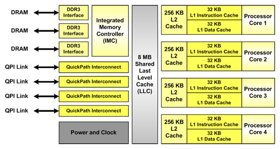
Modern processors typically have two to three levels of cache. Each processor core has private level 1 (L1) data and instruction caches and a L2 combined data+instruction cache. Sometimes, a shared L3 cache is used to serve as an additional buffer between the cache and main memory. The figure below shows the cache hierarchy in a modern processor.

Modern Cache Architectures
To give an idea of typical cache sizes, examples of modern processor caches are given in the table below.
| Vendor and Processor | Cores | L1 cache | L2 cache | L3 cache | Date |
|---|---|---|---|---|---|
| Intel Pentium Dual Core | 2 | I: 32KB D: 32KB | 1MB 8-way set-associative | - | 2006 |
| Intel Xenon Clovertown | 2 | I: 4x 32KB D: 4x 32KB | 2x 4MB | - | January 2007 |
| Intel Xenon 3200 Series | 4 | 2x 4MB | - | January 2007 | |
| AMD Athlon 64 FX | 2 | I: 64KB D: 4KB 2-way set-associative | 1MB 16-way set-associative | - | May 2007 |
| AMD Athlon 64 X2 | 2 | I: 64KB D: 4KB 2-way set-associative | 512KB/1MB 16-way set-associative | 2MB | June 2007 |
| AMD Barcelona | 4 | I: 64KB D: 64KB | 512KB | 2MB | August 2007 |
| Sun Microsystems Ultra Sparc T2 | 8 | I: 16KB D: 8KB | 4MB 8 banks, 4-way set-associative | - | October 2007 |
| Intel Xeon Wolfdale DP | 2 | D: 96KB | 6MB | - | November 2007 |
| Intel Xeon Harpertown | 4 | D: 96KB | 2x 6MB | - | November 2007 |
| AMD Phenom | 4 | I: 64KB D: 64KB | 512KB | 2MB shared | November 2007, March 2008 |
| Intel Core 2 Duo | 2 | I: 32KB D: 32KB | 2-4MB 8-way set-associative | - | 2008 |
| Intel Penryn Wolfdale | 4 | 6-12MB | 6MB | March, August 2008 | |
| Intel Core 2 Quad Yorkfield | 4 | D: 96KB | 12MB | - | March 2008 |
| AMD Toliman | 3 K10 | I: 64KB D: 64KB | 512KB | 2MB shared | April 2008 |
| Azul Systems Vega 3 7300 Series | 864 | 768GB total | - | - | May 2008 |
| IBM RoadRunner | 8+1 | 32KB | 512KB | - | June 2008 |
Write Policy
When the processor issues a write, the write policy used determines how data is transferred between different levels of the memory hierarchy. Each policy has advantages and disadvantages.
Write Hit Policies
Write-through: In a write-through policy, changes written to the cache are immediately propagated to lower levels in the memory hierarchy. [3] Write-back: In a write-back policy, changes written to the cache are only propagated to lower levels when a changed block is evicted from the cache. [3]
Write Miss Policies
Fetch-on-write: In a fetch-on-write policy, a block is fetched from lower levels of memory whenever there is a write miss. This policy usually implies write allocate. [2]
Write-allocate: In a write-allocate policy, a block is brought into the cache the before it is written.[3]
Write-invalidate: In a write-invalidate policy, a written block is marked invalid. [2]
These policies can be combined to form a cohesive cache write policy. For instance, the write-validate policy is formed by the combination of no-fetch-on-write, write allocate, and no-write-invalidate. The write-around policy is formed by the combination of no-fetch-on-write, no-write-allocate, and no-write-invalidate. The write-invalidate policy is formed by the combination of no-fetch-on-write, no-write-allocate, and write-invalidate. [2]
Prefetching
References
1 http://embedded.communities.intel.com/community/en/rovingreporter/blog/tags/GE
2 "Cache write policies and performance," Norman Jouppi, Proc. 20th International Symposium on Computer Architecture (ACM Computer Architecture News 21:2), May 1993, pp. 191-201.
3 textbook