6 Multi: Difference between revisions
No edit summary |
No edit summary |
||
| (7 intermediate revisions by the same user not shown) | |||
| Line 1: | Line 1: | ||
Multi core architecture: The term ‘multicore’ means two or more independent cores. The term ‘architecture’ means the design/layout of a particular idea. Hence the combined term ‘multicore architecture’ simply means the integration of cores and its layout. For e.g. ‘dual core’ means each processor contains 2 independent cores. | |||
NUMA architectures: The term NUMA is an acronym for Non Uniform Memory Access. It is one way of organizing the MIMD (Multiple Instruction Multiple Data: independent processors are connected together to form a multiprocessor system.) architecture. NUMA is also known as distributed shared memory. Each processor has an independent cache, memory and they are connected to a common interconnection network like a crossbar, mesh, hypercube, etc. | |||
A crossbar is a switch which can connect processors to memory in any order. However, it becomes expensive to use, hence as a compromise between crossbar and shared bus sytems, multistage interconnection networks are used (e.g. network on chip interconnects) | |||
**‘Cache’ is a storage device having small memory. Why were caches introduced? [4] | |||
The | **The CPU works at clock frequencies of 3 GHZ and most common RAM speeds are about 400 MHz. Hence, there needs to be a transfer of data to and fro from RAM and CPU. This will increase the latency and CPU will remain idle most times. The main reason of introducing caches was to reduce this latency to access the data from main memory. These small buffers (caches) operate at higher speeds than normal RAM and hence data can be accessed quickly from the cache. | ||
**The cache which is closest to CPU is called Level 1 Cache or L1 cache. It is also known as primary cache. The size is between 8 KB – 128 KB. The next level is L2 cache (secondary cache) whose size is between 256 KB – 1024 KB. If the data that CPU is looking for is not found in registers, it seeks it in L1 cache, if not found, then in L2 cache, then to the main memory, then finally to an external storage device. | |||
**This leads us to the introduction of two new terms: cache hit and cache miss. | |||
**The data searched for by registers, if found in cache, results in cache hit, and if not found in cache, results in cache miss. | |||
**With the introduction of multiple cache levels, it can be individually stated as L1 cache hit/miss, L2 cache hit/miss and so on. | |||
**Most modern computers use the following memory hierarchy. The figure below shows an uni processor memory hierarchy & a recent dual core memory hierarchy | |||
Uni processor memory hierarchy Dual core memory hierarchy | Uni processor memory hierarchy [3] Dual core memory hierarchy [2] | ||
**Previously the processors had an unified L1 cache i.e. data and instruction cache were unified in one. If the Instruction fetch unit wants to fetch data from the cache and the memory unit wants to load an address simultaneously, then the memory operation is given priority and the fetch unit is stalled. Hence, L1 cache was split into L1 data cache (L1 – D) and L1 instruction cache (L1 -I) so that it helps in concurrency. One more advantage is fewer number of ports will be required. | |||
**L2 cache is still unified. As the latency difference between main memory and the fastest cache has become larger, some processors have begun to utilize L3 cache, some don’t. Hence the above figure shows 2 boxes, one which includes L1 and L2, and the other which combines L3 with them. The L3 cache is roughly about 4 MB – 32 MB in size. | |||
L2 cache is still unified. As the latency difference between main memory and the fastest cache has become larger, some processors have begun to utilize L3 cache, some don’t. Hence the figure shows 2 boxes, one which includes L1 and L2, and the other which combines L3 with them. The L3 cache is roughly about 4 MB – 32 MB in size. | |||
In addition to these 3 levels of cache, some | **In addition to these 3 levels of cache, some multicore processors use: Inclusion property, Victim cache, Translation LookAside Buffer, Trace Cache, Smart Cache (Intel) | ||
Inclusion Property: Here, the bigger in size lower level cache (L2) includes all the data of upper level (L1) cache. The advantage of this property is that if a value is not found in the lower level cache, it is guaranteed it is not present in the upper level cache, which reduces the amount of checking. The disadvantage is if L2 cache is smaller in size, most of it contains only L1 cache data and hardly any new data, defeating the purpose of another level of cache altogether. | **Inclusion Property: Here, the bigger in size lower level cache (L2) includes all the data of upper level (L1) cache. The advantage of this property is that if a value is not found in the lower level cache, it is guaranteed it is not present in the upper level cache, which reduces the amount of checking. The disadvantage is if L2 cache is smaller in size, most of it contains only L1 cache data and hardly any new data, defeating the purpose of another level of cache altogether. | ||
A victim cache is a cache used to hold blocks evicted from a CPU cache upon replacement. When main cache evicts a block, the victim cache will take the evicted block. This block is called the victim block. When the main cache misses, it searches the victim cache for recently evicted blocks. So, a hit in victim cache means the main cache doesn’t have to go to the next level of memory. | **A victim cache is a cache used to hold blocks evicted from a CPU cache upon replacement. When main cache evicts a block, the victim cache will take the evicted block. This block is called the victim block. When the main cache misses, it searches the victim cache for recently evicted blocks. So, a hit in victim cache means the main cache doesn’t have to go to the next level of memory. | ||
The TLB is a small cache holding recently used virtual-to-physical address translations. TLB is a hardware cache that sits alongside the L1 instruction and data caches. | **The TLB is a small cache holding recently used virtual-to-physical address translations. TLB is a hardware cache that sits alongside the L1 instruction and data caches. | ||
**The trace cache is located between the decoder unit and the execution unit. Thus the fetch unit grabs data directly from L2 memory cache. | |||
**Intel Advanced Smart Cache is a multi-core optimized cache that improves performance by increasing the probability that each execution core of a dual-core processor can access data from a higher-performance, more-efficient cache subsystem. To accomplish this, Intel Core micro architecture shares the Level 2 (L2) cache between the cores. If one of the cores is inactive, the other core will have access to the full cache. It provides a peak transfer rate of 96 GB/sec (at 3 GHz frequency). | |||
Parameters of a cache: | Parameters of a cache: | ||
** 1. Size: cache data storage. | |||
**2. Associativity: Number of blocks in a set | |||
**3. Block Size: Total number of bytes in a single block. | |||
**A set is a fancy term used for the row of a cache. | |||
PLACEMENT POLICY: The placement policy is the first step in managing a cache. This decides where a block in memory can be placed in the cache. The placement policies are: | |||
The placement policy is the first step in managing a cache. This decides where a block in memory can be placed in the cache. The placement policies are: | |||
1. Direct mapped: If each block has only one place where it can appear in a cache, it is called direct- mapping. It is also known as one way set associative.[6] | |||
**The main memory address (32 bits) is broken down as: (Assumed 8 blocks and 8 lines in cache.) | |||
** | |||
26 bits 3 bits 3 bits | 26 bits 3 bits 3 bits | ||
TAG INDEX OFFSET | TAG INDEX OFFSET | ||
** Number of offset bits = log 2 Block Size | |||
**Number of index bits = log 2 Number of sets | |||
**Number of Tag bits = 32- offset bits- index bits | |||
**Each line has its own tag associated with it. The index tells which row of cache to look at. To search for a word in the cache, compare the tag bits of the address with the tag of the line. If it matches, the block is in the cache. It is a cache hit. Then select the corresponding word from that line. | |||
Each line has its own tag associated with it. The index | |||
2. Fully Associative: If any line can store the contents of any memory location, it is known as fully associative cache. Hence, no index bits are required. | |||
**The main memory address (32 bits) is broken down as: | |||
** | |||
29 bits 3 bits | 29 bits 3 bits | ||
TAG OFFSET | TAG OFFSET | ||
**It is also known as Content Addressable Memory. To search for a word in the cache, compare the tag bits of the address with the tag of all lines in the cache simultaneously. If any one matches, the word is in the cache. Then select the corresponding word from that line. | |||
1. Set Associative: | |||
** | |||
Direct Mapped Fully Associative | Direct Mapped Fully Associative | ||
Advantages: Fast lookup, Less hardware Minimal contention for lines | Advantages: Fast lookup, Less hardware Minimal contention for lines | ||
Disadvantages: Contention for cache lines Maximum Hardware & Cost | Disadvantages: Contention for cache lines Maximum Hardware & Cost | ||
Hence, a compromise between the fully associative cache and the direct mapping technique is made, known as set associative mapping. Almost 90% of the current processors use this mapping. | **Hence, a compromise between the fully associative cache and the direct mapping technique is made, known as set associative mapping. Almost 90% of the current processors use this mapping. | ||
Here the cache is divided into ‘s’ sets, where s is a power of 2. The associativity can be found by using the following relation: | **Here the cache is divided into ‘s’ sets, where s is a power of 2. The associativity can be found by using the following relation: | ||
**Associativity = Cache size/ (Block Size * Number of sets). For an associativity of ‘n’, the cache is ‘n- way’ set associative. | |||
Associativity = Cache size/ (Block Size * | |||
[[Image: Picture15.png]] | |||
**2 way set associative mapping [3] | |||
**Here the cache size is the same, but the index field is 1 bit shorter. Based on the index bits, select a particular set. To search for a word in the cache, compare the tag bits of the address with the tag bits of the line in each set (here 2). If it matches with any one of the tags, it is a cache hit. Else, it is a cache miss and the word has to be fetched from main memory. | |||
Conceptually, the direct mapped and fully associative caches are just "special cases" of the N-way set associative cache. If you make n=1, it becomes a "1-way" set associative cache. i.e. there is only one line per set, which is the same as a direct mapped cache. On the other hand, if you make ‘n’ to be equal to the number of lines in the cache, then you only have one set, containing all of the cache lines, and each and every memory location points to that set. This gives us a fully associative cache. | |||
1. Make small counters per block in a set and the | REPLACEMENT POLICY: This decides which block needs to be evicted to make space available for a new block entry. The replacement policies used are: LRU, Psuedo LRU, FIFO, OPT, random, etc. | ||
2. If there is a cache hit, make the current block’s counter value as 0, which indicates that it is the most recently used one. Increment the counters of other blocks whose | The most commonly used is LRU (Least recently used replacement policy). It works as follows: [3] | ||
3. If there is a cache miss, make the newly allocated block’s counter value as 0 and then increment the counters of all other blocks | ** 1. Make small counters per block in a set and the number of bits in each counter = | ||
log2 (Associativity) | |||
**2. If there is a cache hit, make the current block’s counter value as 0, which indicates that it is the most recently used one. Increment the counters of the other blocks whose counter values are less than the referenced block’s old counter value | |||
**3.If there is a cache miss, make the newly allocated block’s counter value as 0 and then increment the counters of all other blocks | |||
One eg: trace ABCEF | **One eg: trace ABCEF. (0-2 indicate counter numbers) | ||
0 1 2 | 0 1 2 | ||
2 0 | 2 0 | ||
| Line 137: | Line 103: | ||
E | E | ||
**When E came in, the block with the highest count here 2, block A was evicted since it was least recently used and the value of other counters were incremented accordingly. Similarly, when F came in, block B was evicted. | |||
**FIFO policy simply removes the cache block which was brought in earliest in the cache, irrespective of it being least, most recently used. | |||
1. Write Through: Whenever a value is written in the cache, it is immediately written in the next level of memory hierarchy. The main advantage is that both levels have the recent | WRITE POLICY: | ||
**1. Write Through: Whenever a value is written in the cache, it is immediately written in the next level of memory hierarchy. The main advantage is that both levels have the recent updated value at all times. No dirty bit is required. The disadvantage is that since it writes every time, it consumes a lot of bandwidth. A bit stored in the cache can flip its value when struck by alpha particles resulting in soft errors. The effect of this is that the value in the cache is lost. Since, the lower level of cache contains the same updated value, it is safe to discard the block, as it can be easily re fetched. So, only error detection is enough. | |||
2. Write Back: The next level of memory hierarchy is not updated as soon as a value is written in the cache, but is updated only when a block is evicted from the cache. To cope up with the | ** 2. Write Back: The next level of memory hierarchy is not updated as soon as a value is written in the cache, but is updated only when a block is evicted from the cache. To cope up with the issue of having the most recent value, a dirty bit is associated with the cache block. When there is a write to the cache, the dirty bit is set 1. So, if this block were to be evicted, indication of dirty bit being 1, will make the block to be written back to the main memory. When a new block is written in cache, the dirty bit is made 0. Since, lower level of cache does not contain the same updated value, error correction is necessary. | ||
Thus in most processors, L1 cache uses a WT policy and L2 cache uses a WB policy. | **Thus in most processors, L1 cache uses a WT policy and L2 cache uses a WB policy. | ||
Write Allocate policy: On a write miss, the block is brought back into the cache before it is written. A write back policy generally uses write allocate. | **Write Allocate policy: On a write miss, the block is brought back into the cache before it is written. A write back policy generally uses write allocate. | ||
**Write No Allocate Policy: On a write miss, the write is propagated to the lower level of memory hierarchy but it is not brought back into the cache. A write through policy generally uses write no allocate. | |||
RECENT MULTI-CORE ARCHITECTURES: Cores in multi-core systems may implement architectures such as superscalar, VLIW, vector processing, SIMD, or multithreading. | |||
**Super scalar architecture implements Instruction level parallelism within a single processor. A superscalar processor executes more than one instruction during a clock cycle. | |||
**Very long instruction word (VLIW) [7] refers to a CPU architecture designed to take advantage of instruction level parallelism (ILP). It includes out of order execution. It is a type of MIMD. VLIW CPUs offer significant computational power with less hardware complexity (but greater compiler complexity) than is associated with most superscalar CPUs. One VLIW instruction encodes multiple operations; specifically, one instruction encodes at least one operation for each execution unit of the device | |||
**Simultaneous multithreading (SMT) is a technique for improving the overall efficiency of superscalar CPUs with hardware multithreading. SMT permits many independent threads of execution to make better utilization of the resources provided by modern processor architectures. | |||
**The following table shows the type of cache structure used by recent processors. | |||
Company & | |||
Processor # cores L1 cache | |||
Per core L2 cache | |||
Per core L3 Year | |||
Intel Xeon | |||
Clowertown 2 D: 4*32 KB | |||
I: 4*32 KB 2*4096 KB Jan 2007 | |||
Intel Xeon | |||
3200 series 4 2* 4 MB Jan 2007 | |||
AMD | |||
2 | Barcelona 4 D: 64 KB | ||
I: 64 KB 512 KB 2 MB | |||
Shared Aug 2007 | |||
Sun Microsystems | |||
Ultra Sparc T2 8 4 MB | |||
(8 banks) | |||
(16 way assoc.) Oct 2007 | |||
Intel Xeon | |||
Wolfdale DP 2 6 MB Nov 2007 | |||
Intel Xeon | |||
Harpertown 4 2*6 MB Nov 2007 | |||
AMD | |||
Phenom 4 D: 64 KB | |||
I: 64 KB 512 KB 2 MB | |||
Shared Nov 2007 | |||
Mar 2008 | Mar 2008 | ||
Intel Penryn | |||
Wolfdale 6 MiB Mar 2008 | |||
Intel Core 2 Quad | |||
Yorkfield 4 Mar 2008 | |||
AMD Toliman | |||
3 K10 D: 64 KB | |||
I: 64 KB 512 KB 2 MB | |||
Sep 2008 | Shared Apr 2008 | ||
Azul Systems | |||
Vega 3 7300 Series 864 768 GB in all May 2008 | |||
IBM RoadRunner [9] | |||
(# 1 in top500.org for | |||
Fastest computers) Jun 2008 | |||
Nehalem-EP | Free Scale QorIQ [ref 9] | ||
P1, P2, P3, P4, P5 | |||
Power QUICC | |||
8 core | |||
P4080 Jun 2008 | |||
Intel Celeron | |||
Merom- L 64 KB 1 MB | |||
Integrated 2008 | |||
Intel Xeon | |||
Dunnington 4/6 3*3 MB 16 MB Sep 2008 | |||
Intel Xeon | |||
Gainestown 4 4 * 256 KB 8 MB Dec 2008 | |||
2 | AMD Phenom II | ||
Deneb | |||
4 K10 D: 64 KB | |||
I: 64 KB 512 KB 6 MB | |||
Shared Jan 2009 | |||
Nvidia GeForce G 100 Mar 2009 | |||
Intel Celeron | |||
Merom 4 MiB Mar 2009 | |||
Intel | |||
Nehalem- EP 2/4 Mar 2009 | |||
AMD Castillo 2 K10 | |||
Chip | |||
Harvesting D: 64 KB | |||
I: 64 KB 512 KB 6 MB | |||
Shared Jun 2009 | |||
AMD Athlon II | |||
Regor 2 K10 D: 64 KB | |||
I: 64 KB 1024 KB Jun 2009 | |||
Intel Core i5 | |||
Lynnfield 4 MB Sep 2009 | |||
AMD Propus 4 K10 D: 64 KB | |||
I: 64 KB 512 KB Sep 2009 | |||
Intel Core i3 | |||
Clarkdale 2 Jan 2010 | |||
IBM Power 7 Feb 2010 | |||
Intel Xeon | |||
Jasper Forest 4 4 * 256 KB 8 MB 2010 | |||
Intel Xeon | Intel Xeon | ||
Becktown 8 8 * 256 KB 24 MB 2010 | |||
Intel Extreme | |||
Edition Gulftown 6 Mar 2010 | |||
Intel Core i7 | |||
Bloomfield 256 Kb 8 MB | |||
Intel Penryn | |||
QC 4 6-12 MB | |||
Intel Penryn XE | |||
Core 2 Extreme 12 MiB | |||
IBM Cell 8+1 256 KB local | |||
Intel i7 8 8 MB | |||
AMD Athlon 64X2 [15] I: 64 KB | |||
D: 4 KB | |||
Both 2 way | |||
Set assoc 512 KB/1 Mb | |||
16 way set | |||
Assoc. | |||
AMD Athlon 64 FX | |||
I: 64 KB | |||
D: 4 KB | |||
Both 2 way | |||
Set assoc 1 Mb | |||
16 way set | |||
Assoc. | |||
Sempron sockets 754 | |||
And AM2 | |||
I: 64 KB | |||
D: 4 KB | |||
Both 2 way | |||
Set assoc 1 Mb | |||
16 way set | |||
Assoc. | |||
Intel Pentium D | |||
(150 KB trace cache) D: 16 KB | |||
4 way set assoc 1 MB/2 MB | |||
Intel Core 2 Duo | |||
(150 KB trace cache) I: 32 KB | |||
D: 32 KB 2/4 MB | |||
8 way set assoc | |||
Intel Pentium | |||
Dual Core | |||
(150 KB trace cache) I: 32 KB | |||
D: 32 KB 1 MB | |||
8 way set assoc. | |||
For recent NUMA architectures: | |||
Bloomfield | |||
4 | |||
Core 2 | |||
256 | |||
8 | |||
32 | |||
1. 4 Opteron 875 dual core processors: 1 L1- D cache per core (2 per socket), size: 65 KB | |||
: 1 L1- I cache per core, size: 65 KB | |||
: 1 L2 cache per core (2 per socket), size: 1MB | |||
2. AMD Hammer: L1: 128 KB, 2 way set assoc. | |||
L2: 1 MB | |||
It also uses a large TLB and a victim cache | |||
3. Altix: The Altix UV supercomputer architecture combines a development of the NUMAlink interconnect used in the Altix 4000 (NUMAlink 5) with 4/6/8-core "Nehalem-EX" Intel Xeon processors. Altix UV systems run either SuSE Linux Enterprise Server or Red Hat Enterprise Linux, and scale from 32 to 2,048 cores with support for up to 16 TB of shared memory in a single system. It came in the end of 2009. | |||
**Other examples are: IBM p690, SGI Origin. Here are two different structures. | |||
**Tilera TILE 64 consists of a mesh network of 64 tiles. It is based on VLIW instruction set. Each of the cores (tile) has its own L1 and L2 cache plus an overall virtual L3 cache, having mutual inclusion property. It was developed in 2007 | |||
**Tilera, TILE- Gx is a future multi core processor consisting of a mesh network of 100 cores. It is a 64 bit core (3 issue) | |||
**L1- I: 32 KB/ core, L1- D: 32 KB/ core, L2: 256 KB/ core, L3: 26 MB/ chip | |||
Write Policies used in recent multi core architectures: | |||
** 1. Intel Pentium Processors: [10] Mainly 2 bits control the cache. CD (cache disable) and NW (not write through) | |||
**CD= 1, cache disabled CD=0, enables the cache | |||
**NW= 0: Write Through, NW=1: Write Back | |||
**A WB line is always fetched into the cache if a cache miss occurs. | |||
**A WT line is not fetched into the cache on a write miss. For the Pentium Pro processor, a WT hit to the L1 cache updates the L1 cache. A WT hit to L2 cache invalidates the L2 cache. | |||
**A WP (Write Protected) line is cacheable, but a write to it cannot modify the cache line. A WP line is not fetched into the cache on a write miss. For the Pentium Pro processor, a WP hit to the L2 cache invalidates the line in the L2 cache. | |||
**An UC (Uncacheable) line is not put into the cache. A UC hit to the L1 or L2 cache invalidates the entry. | |||
**Cache consistency: MESI (Modified, Exclusive, Shared, Invalid) policy is used. | |||
1. Intel IA 32 IA64 architecture: [12] In IA 32, the number of processor sharing the cache is one plus value represented by CPUID.4.EAX [25:14] | |||
**Write combining: Successive writes to the same cache line are combined. | |||
**Write collapsing: Successive writes to the same bytes result in only the last write being visible. | |||
**Weakly ordered: No ordering is preserved between WC stores or between other loads or stores. | |||
** Uncacheable & Write No Allocate: Stored data is written around the cache and it uses Write No Allocate. | |||
**Non-temporal: Data which is referenced once and not reused in the immediate future | |||
** If the programmer specifies a non-temporal store to UC or WP memory types, then the store behaves like an uncacheable store. There is no conflict if a non temporal store to WC is specified. If the programmer specifies a non-temporal store to WB or WT memory types, and if the data is in the cache, will ensure consistency. However, if it is a miss, the transaction is subject to all WC memory semantics, which will not write allocate. | |||
2. Celeron and Xeon based on Netburst microarchitecture (i.e. based on Pentium 4) will have the same specs as Pentium 4 but with different L2 cache size, while Celeron and Xeon based on Core microarchitecture (i.e. based on Core 2 Duo) will have the same specs as Core 2 Duo but with different L2 cache size. | |||
**Intel Xeon Clowertown: L1: 8 way associative & L2: 16 way associative **Intel Celeron using Intel Core 2 architecture: L2: 16 way associative ** L1- D: 8 way associative ** L1- I: 8 way associative ** 16 entry DTLB | |||
**4. Intel RAID: These use Write Back policy. | |||
**5. Intel Core microarchitecture uses FIFO replacement policy. | |||
**6. AMD uses cache exclusion unlike Intel’s cache inclusion | |||
** 7. In general, WT invalidate protocols gives better performance than WB- MESI protocols. But most modern processors use WB policy. | |||
References: | |||
** [1]: http://www.buzzle.com/articles/basics-of-dual-core-process-computer.html | |||
** [2]: Fundamentals of Parallel Computer Architecture by Yan Solihin | |||
Technology: | ** [3]: Computer Design & Technology- Eric Rotenberg. | ||
** [4]: http://www.karbosguide.com/books/pcarchitecture/chapter10.htm | |||
** [5]: http://www.real-knowledge.com/memory.htm | |||
** [6]: http://www.pcguide.com/ref/mbsys/cache/funcMapping-c.html | |||
** [7]:http://en.wikipedia.org/wiki/Very_Long_Instruction_Word | |||
** [8]: http://en.wikipedia.org/wiki/CPU_cache#Multi-level_caches | |||
** [9]: http://en.wikipedia.org/wiki/Power_Architecture | |||
** [10]: http://en.wikipedia.org/wiki/Multi-core_processor | |||
** [11]: http://download.intel.com/design/archives/processors/pro/docs/24269001.pdf | |||
** [12]: http://www.intel.com/Assets/PDF/manual/248966.pdf | |||
** [13]: http://www.hardwaresecrets.com/article/366/2 | |||
** [14]: http://www.intel.com/design/intarch/papers/cache6.pdf | |||
** [15]: http://www.hardwaresecrets.com/article/481/9 | |||
Latest revision as of 07:06, 22 February 2010
Multi core architecture: The term ‘multicore’ means two or more independent cores. The term ‘architecture’ means the design/layout of a particular idea. Hence the combined term ‘multicore architecture’ simply means the integration of cores and its layout. For e.g. ‘dual core’ means each processor contains 2 independent cores.
NUMA architectures: The term NUMA is an acronym for Non Uniform Memory Access. It is one way of organizing the MIMD (Multiple Instruction Multiple Data: independent processors are connected together to form a multiprocessor system.) architecture. NUMA is also known as distributed shared memory. Each processor has an independent cache, memory and they are connected to a common interconnection network like a crossbar, mesh, hypercube, etc.
A crossbar is a switch which can connect processors to memory in any order. However, it becomes expensive to use, hence as a compromise between crossbar and shared bus sytems, multistage interconnection networks are used (e.g. network on chip interconnects)
- ‘Cache’ is a storage device having small memory. Why were caches introduced? [4]
**The CPU works at clock frequencies of 3 GHZ and most common RAM speeds are about 400 MHz. Hence, there needs to be a transfer of data to and fro from RAM and CPU. This will increase the latency and CPU will remain idle most times. The main reason of introducing caches was to reduce this latency to access the data from main memory. These small buffers (caches) operate at higher speeds than normal RAM and hence data can be accessed quickly from the cache.
- The cache which is closest to CPU is called Level 1 Cache or L1 cache. It is also known as primary cache. The size is between 8 KB – 128 KB. The next level is L2 cache (secondary cache) whose size is between 256 KB – 1024 KB. If the data that CPU is looking for is not found in registers, it seeks it in L1 cache, if not found, then in L2 cache, then to the main memory, then finally to an external storage device.
- This leads us to the introduction of two new terms: cache hit and cache miss.
- The data searched for by registers, if found in cache, results in cache hit, and if not found in cache, results in cache miss.
- With the introduction of multiple cache levels, it can be individually stated as L1 cache hit/miss, L2 cache hit/miss and so on.
**Most modern computers use the following memory hierarchy.  The figure below shows an uni processor memory hierarchy & a recent dual core memory hierarchy

       Uni processor memory hierarchy [3]	                  Dual core memory hierarchy [2]
- Previously the processors had an unified L1 cache i.e. data and instruction cache were unified in one. If the Instruction fetch unit wants to fetch data from the cache and the memory unit wants to load an address simultaneously, then the memory operation is given priority and the fetch unit is stalled. Hence, L1 cache was split into L1 data cache (L1 – D) and L1 instruction cache (L1 -I) so that it helps in concurrency. One more advantage is fewer number of ports will be required.
- L2 cache is still unified. As the latency difference between main memory and the fastest cache has become larger, some processors have begun to utilize L3 cache, some don’t. Hence the above figure shows 2 boxes, one which includes L1 and L2, and the other which combines L3 with them. The L3 cache is roughly about 4 MB – 32 MB in size.
- In addition to these 3 levels of cache, some multicore processors use: Inclusion property, Victim cache, Translation LookAside Buffer, Trace Cache, Smart Cache (Intel)
- Inclusion Property: Here, the bigger in size lower level cache (L2) includes all the data of upper level (L1) cache. The advantage of this property is that if a value is not found in the lower level cache, it is guaranteed it is not present in the upper level cache, which reduces the amount of checking. The disadvantage is if L2 cache is smaller in size, most of it contains only L1 cache data and hardly any new data, defeating the purpose of another level of cache altogether.
- A victim cache is a cache used to hold blocks evicted from a CPU cache upon replacement. When main cache evicts a block, the victim cache will take the evicted block. This block is called the victim block. When the main cache misses, it searches the victim cache for recently evicted blocks. So, a hit in victim cache means the main cache doesn’t have to go to the next level of memory.
- The TLB is a small cache holding recently used virtual-to-physical address translations. TLB is a hardware cache that sits alongside the L1 instruction and data caches.
- The trace cache is located between the decoder unit and the execution unit. Thus the fetch unit grabs data directly from L2 memory cache.
- Intel Advanced Smart Cache is a multi-core optimized cache that improves performance by increasing the probability that each execution core of a dual-core processor can access data from a higher-performance, more-efficient cache subsystem. To accomplish this, Intel Core micro architecture shares the Level 2 (L2) cache between the cores. If one of the cores is inactive, the other core will have access to the full cache. It provides a peak transfer rate of 96 GB/sec (at 3 GHz frequency).
Parameters of a cache:
- 1. Size: cache data storage.
- 2. Associativity: Number of blocks in a set
- 3. Block Size: Total number of bytes in a single block.
- A set is a fancy term used for the row of a cache.
PLACEMENT POLICY: The placement policy is the first step in managing a cache. This decides where a block in memory can be placed in the cache. The placement policies are:
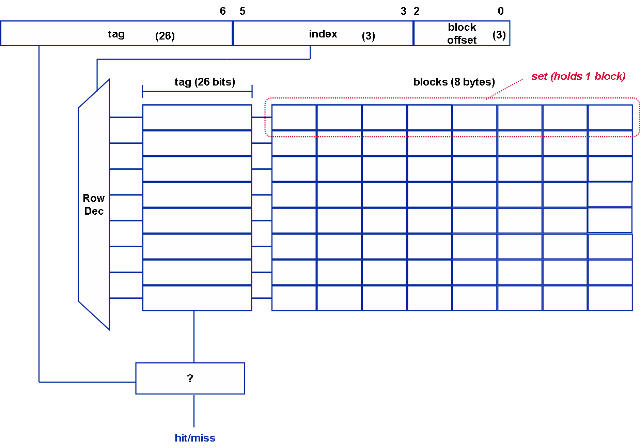
1. Direct mapped: If each block has only one place where it can appear in a cache, it is called direct- mapping. It is also known as one way set associative.[6]
- The main memory address (32 bits) is broken down as: (Assumed 8 blocks and 8 lines in cache.)
26 bits 3 bits 3 bits TAG INDEX OFFSET
** Number of offset bits = log 2 Block Size
**Number of index bits = log 2 Number of sets **Number of Tag bits = 32- offset bits- index bits
- Each line has its own tag associated with it. The index tells which row of cache to look at. To search for a word in the cache, compare the tag bits of the address with the tag of the line. If it matches, the block is in the cache. It is a cache hit. Then select the corresponding word from that line.
2. Fully Associative: If any line can store the contents of any memory location, it is known as fully associative cache. Hence, no index bits are required.
- The main memory address (32 bits) is broken down as:
29 bits 3 bits
TAG OFFSET
- It is also known as Content Addressable Memory. To search for a word in the cache, compare the tag bits of the address with the tag of all lines in the cache simultaneously. If any one matches, the word is in the cache. Then select the corresponding word from that line.
1. Set Associative:
Direct Mapped Fully Associative Advantages: Fast lookup, Less hardware Minimal contention for lines Disadvantages: Contention for cache lines Maximum Hardware & Cost
- Hence, a compromise between the fully associative cache and the direct mapping technique is made, known as set associative mapping. Almost 90% of the current processors use this mapping.
- Here the cache is divided into ‘s’ sets, where s is a power of 2. The associativity can be found by using the following relation:
- Associativity = Cache size/ (Block Size * Number of sets). For an associativity of ‘n’, the cache is ‘n- way’ set associative.

**2 way set associative mapping [3]
- Here the cache size is the same, but the index field is 1 bit shorter. Based on the index bits, select a particular set. To search for a word in the cache, compare the tag bits of the address with the tag bits of the line in each set (here 2). If it matches with any one of the tags, it is a cache hit. Else, it is a cache miss and the word has to be fetched from main memory.
Conceptually, the direct mapped and fully associative caches are just "special cases" of the N-way set associative cache. If you make n=1, it becomes a "1-way" set associative cache. i.e. there is only one line per set, which is the same as a direct mapped cache. On the other hand, if you make ‘n’ to be equal to the number of lines in the cache, then you only have one set, containing all of the cache lines, and each and every memory location points to that set. This gives us a fully associative cache.
REPLACEMENT POLICY: This decides which block needs to be evicted to make space available for a new block entry. The replacement policies used are: LRU, Psuedo LRU, FIFO, OPT, random, etc. The most commonly used is LRU (Least recently used replacement policy). It works as follows: [3]
- 1. Make small counters per block in a set and the number of bits in each counter =
log2 (Associativity)
- 2. If there is a cache hit, make the current block’s counter value as 0, which indicates that it is the most recently used one. Increment the counters of the other blocks whose counter values are less than the referenced block’s old counter value
- 3.If there is a cache miss, make the newly allocated block’s counter value as 0 and then increment the counters of all other blocks
- One eg: trace ABCEF. (0-2 indicate counter numbers)
0 1 2 2 0 B 1 A 0 C 1 B 2 A 1 C 2 B 0 E 2 C 0 F 1 E
- When E came in, the block with the highest count here 2, block A was evicted since it was least recently used and the value of other counters were incremented accordingly. Similarly, when F came in, block B was evicted.
- FIFO policy simply removes the cache block which was brought in earliest in the cache, irrespective of it being least, most recently used.
WRITE POLICY:
- 1. Write Through: Whenever a value is written in the cache, it is immediately written in the next level of memory hierarchy. The main advantage is that both levels have the recent updated value at all times. No dirty bit is required. The disadvantage is that since it writes every time, it consumes a lot of bandwidth. A bit stored in the cache can flip its value when struck by alpha particles resulting in soft errors. The effect of this is that the value in the cache is lost. Since, the lower level of cache contains the same updated value, it is safe to discard the block, as it can be easily re fetched. So, only error detection is enough.
- 2. Write Back: The next level of memory hierarchy is not updated as soon as a value is written in the cache, but is updated only when a block is evicted from the cache. To cope up with the issue of having the most recent value, a dirty bit is associated with the cache block. When there is a write to the cache, the dirty bit is set 1. So, if this block were to be evicted, indication of dirty bit being 1, will make the block to be written back to the main memory. When a new block is written in cache, the dirty bit is made 0. Since, lower level of cache does not contain the same updated value, error correction is necessary.
- Thus in most processors, L1 cache uses a WT policy and L2 cache uses a WB policy.
- Write Allocate policy: On a write miss, the block is brought back into the cache before it is written. A write back policy generally uses write allocate.
- Write No Allocate Policy: On a write miss, the write is propagated to the lower level of memory hierarchy but it is not brought back into the cache. A write through policy generally uses write no allocate.
RECENT MULTI-CORE ARCHITECTURES: Cores in multi-core systems may implement architectures such as superscalar, VLIW, vector processing, SIMD, or multithreading.
- Super scalar architecture implements Instruction level parallelism within a single processor. A superscalar processor executes more than one instruction during a clock cycle.
- Very long instruction word (VLIW) [7] refers to a CPU architecture designed to take advantage of instruction level parallelism (ILP). It includes out of order execution. It is a type of MIMD. VLIW CPUs offer significant computational power with less hardware complexity (but greater compiler complexity) than is associated with most superscalar CPUs. One VLIW instruction encodes multiple operations; specifically, one instruction encodes at least one operation for each execution unit of the device
- Simultaneous multithreading (SMT) is a technique for improving the overall efficiency of superscalar CPUs with hardware multithreading. SMT permits many independent threads of execution to make better utilization of the resources provided by modern processor architectures.
- The following table shows the type of cache structure used by recent processors.
Company &
Processor # cores L1 cache
Per core L2 cache
Per core L3 Year
Intel Xeon
Clowertown 2 D: 4*32 KB
I: 4*32 KB 2*4096 KB Jan 2007
Intel Xeon
3200 series 4 2* 4 MB Jan 2007
AMD
Barcelona 4 D: 64 KB
I: 64 KB 512 KB 2 MB
Shared Aug 2007
Sun Microsystems
Ultra Sparc T2 8 4 MB
(8 banks)
(16 way assoc.) Oct 2007
Intel Xeon
Wolfdale DP 2 6 MB Nov 2007
Intel Xeon
Harpertown 4 2*6 MB Nov 2007
AMD
Phenom 4 D: 64 KB
I: 64 KB 512 KB 2 MB
Shared Nov 2007
Mar 2008
Intel Penryn
Wolfdale 6 MiB Mar 2008
Intel Core 2 Quad
Yorkfield 4 Mar 2008
AMD Toliman
3 K10 D: 64 KB
I: 64 KB 512 KB 2 MB
Shared Apr 2008
Azul Systems
Vega 3 7300 Series 864 768 GB in all May 2008
IBM RoadRunner [9]
(# 1 in top500.org for
Fastest computers) Jun 2008
Free Scale QorIQ [ref 9]
P1, P2, P3, P4, P5
Power QUICC
8 core
P4080 Jun 2008
Intel Celeron
Merom- L 64 KB 1 MB
Integrated 2008
Intel Xeon
Dunnington 4/6 3*3 MB 16 MB Sep 2008
Intel Xeon
Gainestown 4 4 * 256 KB 8 MB Dec 2008
AMD Phenom II
Deneb
4 K10 D: 64 KB
I: 64 KB 512 KB 6 MB
Shared Jan 2009
Nvidia GeForce G 100 Mar 2009
Intel Celeron
Merom 4 MiB Mar 2009
Intel
Nehalem- EP 2/4 Mar 2009
AMD Castillo 2 K10
Chip
Harvesting D: 64 KB
I: 64 KB 512 KB 6 MB
Shared Jun 2009
AMD Athlon II
Regor 2 K10 D: 64 KB
I: 64 KB 1024 KB Jun 2009
Intel Core i5
Lynnfield 4 MB Sep 2009
AMD Propus 4 K10 D: 64 KB
I: 64 KB 512 KB Sep 2009
Intel Core i3
Clarkdale 2 Jan 2010
IBM Power 7 Feb 2010
Intel Xeon
Jasper Forest 4 4 * 256 KB 8 MB 2010
Intel Xeon
Becktown 8 8 * 256 KB 24 MB 2010
Intel Extreme
Edition Gulftown 6 Mar 2010
Intel Core i7
Bloomfield 256 Kb 8 MB
Intel Penryn
QC 4 6-12 MB
Intel Penryn XE
Core 2 Extreme 12 MiB
IBM Cell 8+1 256 KB local
Intel i7 8 8 MB
AMD Athlon 64X2 [15] I: 64 KB
D: 4 KB
Both 2 way
Set assoc 512 KB/1 Mb
16 way set
Assoc.
AMD Athlon 64 FX
I: 64 KB
D: 4 KB
Both 2 way
Set assoc 1 Mb
16 way set
Assoc.
Sempron sockets 754
And AM2
I: 64 KB
D: 4 KB
Both 2 way
Set assoc 1 Mb
16 way set
Assoc.
Intel Pentium D
(150 KB trace cache) D: 16 KB
4 way set assoc 1 MB/2 MB
Intel Core 2 Duo
(150 KB trace cache) I: 32 KB
D: 32 KB 2/4 MB
8 way set assoc
Intel Pentium
Dual Core
(150 KB trace cache) I: 32 KB
D: 32 KB 1 MB
8 way set assoc.
For recent NUMA architectures:
1. 4 Opteron 875 dual core processors: 1 L1- D cache per core (2 per socket), size: 65 KB
: 1 L1- I cache per core, size: 65 KB : 1 L2 cache per core (2 per socket), size: 1MB
2. AMD Hammer: L1: 128 KB, 2 way set assoc.
                                  L2: 1 MB
                                  It also uses a large TLB and a victim cache
3. Altix: The Altix UV supercomputer architecture combines a development of the NUMAlink interconnect used in the Altix 4000 (NUMAlink 5) with 4/6/8-core "Nehalem-EX" Intel Xeon processors. Altix UV systems run either SuSE Linux Enterprise Server or Red Hat Enterprise Linux, and scale from 32 to 2,048 cores with support for up to 16 TB of shared memory in a single system. It came in the end of 2009.
- Other examples are: IBM p690, SGI Origin. Here are two different structures.
- Tilera TILE 64 consists of a mesh network of 64 tiles. It is based on VLIW instruction set. Each of the cores (tile) has its own L1 and L2 cache plus an overall virtual L3 cache, having mutual inclusion property. It was developed in 2007
- Tilera, TILE- Gx is a future multi core processor consisting of a mesh network of 100 cores. It is a 64 bit core (3 issue)
- L1- I: 32 KB/ core, L1- D: 32 KB/ core, L2: 256 KB/ core, L3: 26 MB/ chip
Write Policies used in recent multi core architectures:
- 1. Intel Pentium Processors: [10] Mainly 2 bits control the cache. CD (cache disable) and NW (not write through)
- CD= 1, cache disabled CD=0, enables the cache
- NW= 0: Write Through, NW=1: Write Back
- A WB line is always fetched into the cache if a cache miss occurs.
- A WT line is not fetched into the cache on a write miss. For the Pentium Pro processor, a WT hit to the L1 cache updates the L1 cache. A WT hit to L2 cache invalidates the L2 cache.
- A WP (Write Protected) line is cacheable, but a write to it cannot modify the cache line. A WP line is not fetched into the cache on a write miss. For the Pentium Pro processor, a WP hit to the L2 cache invalidates the line in the L2 cache.
- An UC (Uncacheable) line is not put into the cache. A UC hit to the L1 or L2 cache invalidates the entry.
- Cache consistency: MESI (Modified, Exclusive, Shared, Invalid) policy is used.
1. Intel IA 32 IA64 architecture: [12] In IA 32, the number of processor sharing the cache is one plus value represented by CPUID.4.EAX [25:14]
**Write combining: Successive writes to the same cache line are combined.
**Write collapsing: Successive writes to the same bytes result in only the last write being visible.
**Weakly ordered: No ordering is preserved between WC stores or between other loads or stores.
** Uncacheable & Write No Allocate: Stored data is written around the cache and it uses Write No Allocate.
**Non-temporal: Data which is referenced once and not reused in the immediate future
** If the programmer specifies a non-temporal store to UC or WP memory types, then the store behaves like an uncacheable store. There is no conflict if a non temporal store to WC is specified. If the programmer specifies a non-temporal store to WB or WT memory types, and if the data is in the cache, will ensure consistency. However, if it is a miss, the transaction is subject to all WC memory semantics, which will not write allocate.
2. Celeron and Xeon based on Netburst microarchitecture (i.e. based on Pentium 4) will have the same specs as Pentium 4 but with different L2 cache size, while Celeron and Xeon based on Core microarchitecture (i.e. based on Core 2 Duo) will have the same specs as Core 2 Duo but with different L2 cache size.
- Intel Xeon Clowertown: L1: 8 way associative & L2: 16 way associative **Intel Celeron using Intel Core 2 architecture: L2: 16 way associative ** L1- D: 8 way associative ** L1- I: 8 way associative ** 16 entry DTLB
- 4. Intel RAID: These use Write Back policy.
- 5. Intel Core microarchitecture uses FIFO replacement policy.
**6. AMD uses cache exclusion unlike Intel’s cache inclusion
- 7. In general, WT invalidate protocols gives better performance than WB- MESI protocols. But most modern processors use WB policy.
References:
- [1]: http://www.buzzle.com/articles/basics-of-dual-core-process-computer.html
- [2]: Fundamentals of Parallel Computer Architecture by Yan Solihin
- [3]: Computer Design & Technology- Eric Rotenberg.
- [4]: http://www.karbosguide.com/books/pcarchitecture/chapter10.htm
- [5]: http://www.real-knowledge.com/memory.htm
- [6]: http://www.pcguide.com/ref/mbsys/cache/funcMapping-c.html
- [7]:http://en.wikipedia.org/wiki/Very_Long_Instruction_Word
- [8]: http://en.wikipedia.org/wiki/CPU_cache#Multi-level_caches
- [9]: http://en.wikipedia.org/wiki/Power_Architecture
- [10]: http://en.wikipedia.org/wiki/Multi-core_processor
- [11]: http://download.intel.com/design/archives/processors/pro/docs/24269001.pdf
- [12]: http://www.intel.com/Assets/PDF/manual/248966.pdf
- [13]: http://www.hardwaresecrets.com/article/366/2
- [14]: http://www.intel.com/design/intarch/papers/cache6.pdf
- [15]: http://www.hardwaresecrets.com/article/481/9